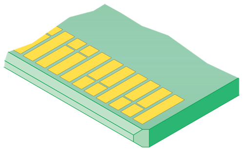
Dual Row Edge Card contacts mate with gold pads on the mating card. Image courtesy of Sullins
Most people think of edge card connectors as being the Neanderthals of the connector industry; old, primitive and crude. I disagree with that and will show you that edge card connectors have evolved rapidly and that you will find them in almost every electronic device, even the fastest ones.
Edge card connectors are famous for being cost effective and inexpensive for connector companies to tool. Many standards are built around edge cards, so there are a host of vendors around the world who can make them, assuring maximum competition and lowest prices to the consumer.
You should, however, be aware of some of the limitations of edge card connectors so you use them properly in your system designs.
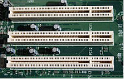
3 PCI slots in a typical PC bus configuration
Photo courtesy of Wikipedia
Edge card connectors are sometimes referred to as “one-piece” connectors because the mating half consists of gold pads on the printed circuit board. This makes them best suited for applications with a limited number of signal paths that can fit into a single row of contacts mating with each side of the plug-in card. Typical high-volume applications in the past have been add-in cards for personal computers and servers. Edge card configurations are especially favored for bused connections where traces on the motherboard connect to a number of expansion slots. PCI (Peripheral Computer Interface) and its many offshoots have been the most common bus systems. This standard was developed by Intel for the IBM PC to connect CPU (Central Processor Unit) with a number of peripheral cards that provide connections for I/O ports to support printers, wireless links, graphic cards, sound cards, disk drives, etc.
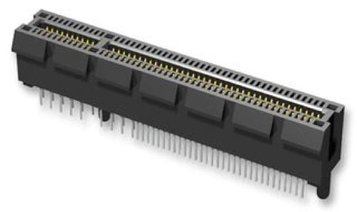
PCI Express Connector
Photo courtesy of Samtec
Parallel bus architectures require that all the signal bits on parallel traces arrive at the receiver before the receiver reads them. This requirement demands that all the signal paths within a group be as close to the same electrical length as possible. The more precisely that this can be controlled, the fewer clock cycles are required and faster the data rate can be.
Layout is also very simple with lots of parallel signal paths on a single layer of the motherboard. A key advantage of systems like this is that the printed circuit boards can be simple and do not need many layers. These cards and motherboards can be designed with 6-8 signal layers, keeping cost low. The tolerances are also generous, making this a great format for high volume, low cost commodity products.
Bussing parallel traces across multiple expansion slots does limit the system speed. An electrical stub is created where each connector “Ts” off of the bus. This stub reflects energy back onto the bussed lines, degrading signal integrity and creating crosstalk. Transmit and receive semiconductors are designed to deal with this higher level of interference, but it does limit the overall transmission speed of the system. PCI, for example, is a 32 bit or 64 bit wide bus structure, initially running at 33 MHz. Over the years, this parallel architecture has evolved to offer bit rates up to 533 MHz for PCI-X 2.0. Just to get you calibrated, today’s serial architectures have bit rates in the range of 25 Gbps, so you can see that bus structures are slow. A 64 bit wide bus requires 64 signal pins plus additional pins for grounds, control signals and power, making these edge card connectors long, eating up precious motherboard space.
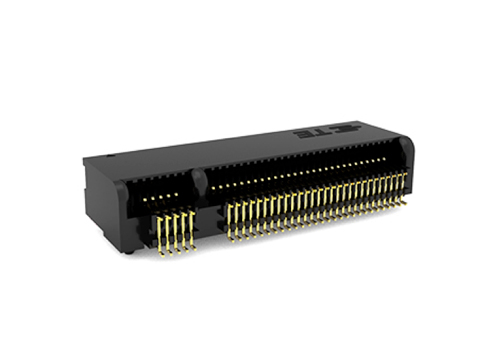
TE M.2 NGFF (Next Generation Form Factor) right angle edge card connector further shrinks the edge card form factor.
To deal with these limitations, the industry, lead by Intel, developed a serial version called PCI Express which kept the edge card format, but uses serial lanes, composed of two differential pairs, one transmitting, the other receiving. Unlike the PCI where a conductor touches each slot, the PCIe traces get an express route directly from the transmitter to the receiver without touching any other slots. This cleaner signal path enables the individual pair to operate at higher frequency, increasing bandwidth. At the connector interface, each signal pair is flanked by a pair of ground pins, further electrically isolating the signals and controlling crosstalk.
PCIe 4.0 now offers 15.7 Gbps per lane, supporting the high performance needed for today’s servers. One nice thing about this kind of serial architecture is that this physical structure can serve not only PCIe, but other serial architectures like SATA and USB as well. Specific pairs can be designated for the mix of protocols that best serves the system requirements.
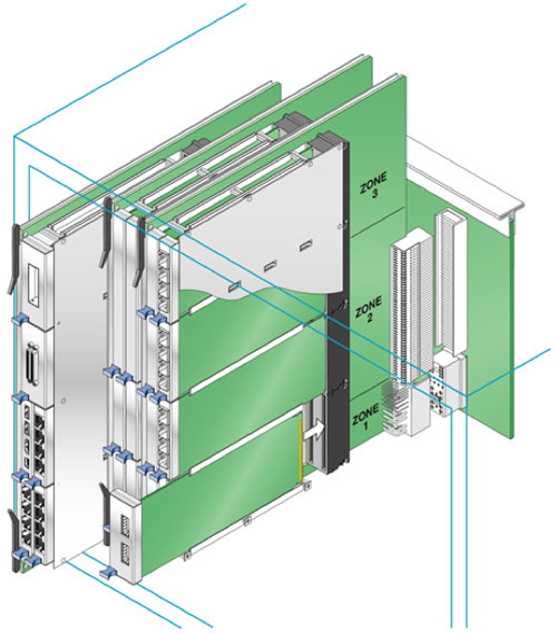
Up to eight standard AMCs (Advanced Mezzanine Cards) can hot plug into a standard ATCA card.
Image by Cleaver Brinkerhoff
Edge card connectors were traditionally mated to expansion cards perpendicular to the motherboard. As the PC has been replaced by smaller form factors like laptops, we often now see right angle edge card connectors supporting horizontal expansion slots parallel to the motherboard. Functions are the same as the vertical edge card connectors, but more friendly to the mobile form factor.
ATCA (Advanced Telecommunication Computer Architecture) from PICMG (PCI Industrial Computer Interface Group) uses this edge card concept in a right angle configuration to support AMCs (Advanced Mezzanine Cards). These electrically tuned connectors are designed to support 25 Gbps, supporting nearly every high speed IO interface using a convenient card about twice the size of a credit card. This versatile interface now supports processors, IO, storage (either semiconductors or rotating disk drives,) and banks of DSP (Digital Signal Processing) chips that enable modern telecommunication systems with sophisticated functionality in a convenient, flexible form factor. AMC cards can be hot swapped, not interrupting system functions as cards are added, removed or upgraded in the field by untrained operators.
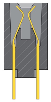
The AMC standard has uniquely designed gold pad configurations to facilitate this hot swap. By splitting gold pads, they are able to achieve three mating levels for ground, signal and enable functions.
Advanced MC cards split pads for sequenced mating. Image by Cleaver Brinkerhoff
Mechanically, edge card connectors do have some other limitations. Because you are mating to gold pads on the plug in cards, cycle life is typically less than you find with two-piece connectors where metal pins or blades mate with nicely formed metal springs on the mating connectors. Edge cards are typically used where less than 200 mating cycles are needed during the lifetime of the connector.
The second limitation of edge cards is that the mating PCB thickness is limited. An edge card designed to mate with a board that is 0.062 in. thick, for example will not work with a thinner 0.032 in. or thicker 0.093 in. board. PCIe and AMC cards are limited to 1 mm (0.040 in.) thick cards. This limitation dictates the number of signal layers on the pluggable card. In contrast, 2 piece pin-and-socket connectors allow thick or thin boards to be used in the same slot.
Typical Cantilever edge card contact beams provide a gentle mating interface. Image by Cleaver Brinkerhoff
The third limitation of edge card connectors is length/density. Because it is a dual row connector with one row of contacts mating to each side of the plug-in card, as you add contacts or lanes, you need to have a longer connector body. For example, a PCI 120 pin connector tops out at 85 mm long (about 12 diff pairs per inch) and PCIe x16 connector is 89 mm long. These are not dense connectors.
Traditional backplane connectors, as a comparison, can offer 40-80 differential pairs per inch of connector length. It is possible to compress the contact pitch on edge cards. For many years, standard edge cards for PCI and other protocols used a 1.27 mm (0.050 in.) pitch. PCI Express form factors have tightened the pitch to 1 mm initially, later introducing PCIe Gen 2 with 0.8 mm version, and even down to 0.5 mm pitch for the M-2 connector family.
One of the design changes needed to achieve the finer pitch is to change the orientation of the contact in the slot. The older edge card connectors mated on the flat, smooth side of the contact. This configuration provided a gentle spring and the mating point was formed into a smooth dome, ensuring long mating life. These contacts were typically all stamped from a single strip of material in a simple, high-speed die. Stations in the die form the strip into the final contact shape. A strip of contacts could be mass inserted into the plastic housing in one motion, making these connectors simple and cost effective to manufacture.
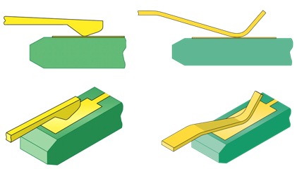
Blanked and coined contact mating, left, and flat stamped contact mates on the sweet side.
Illustrations courtesy of Cleaver Brinkerhoff
To achieve the tighter pitch, a different manufacturing method evolved. The contacts are blanked and then stitched into the plastic, one or two at a time, with the sheared edge mating to the gold pad on the card. This configuration creates a more rigid spring, and additional coining is necessary in the die to ensure that the contact mates smoothly with the gold pad. This would seem to be a bad thing, but in fact, electrical performance became better because adjacent contacts can be electrically broadside coupled with the energy actually flowing in the space between the two contacts of the differential pair. By designating one or two pins between signal pairs as grounds, crosstalk is reduced, and the signals can run at higher data rates.
SFP connector and cages enable front panel pluggable modules
Image courtesy of Leoco
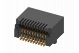
The stitched, blanked and coined contact approach is used in many different configurations of edge card connectors. The stampings can have right angle bends, for example, enabling right angle configurations well-suited for tighter pitch connectors used for memory cards like the SD cards used in laptops, cameras and other mobile devices. The same principle is employed for high speed connectors used in pluggable devices like SFP, QSFP and other similar formats. These connectors are tuned to achieve up to 28 Gbps performance for each differential pair.
So, as you can see, the venerable edge card concept has evolved over the years to become denser, smaller and electrically faster with successive generations of designs. When you realize that the pluggable modules like SFP and QSFP now support state-of-the-art optical transceivers, it seems that these advanced edge card designs will continue to have a long life in the future.
The post Can edge card connectors be exciting? appeared first on Connector Tips.
Filed Under: Connectors (electrical) • crimp technologies, Connector Tips