By Jerome Johnston
Power system designers are always seeking higher power capability built on smaller footprints. This is especially true for datacenter servers and LTE basestations that support high current loads from increasingly power hungry FPGAs, ASICs and microprocessors. To reach higher output currents, multi-phase systems are being used more and more. To get higher current levels out of parts with smaller footprints, system designers are moving away from discrete power solutions in favor of power modules. That’s because modules offer a popular alternative to complex power designs and the printed circuit board (PCB) layout issues associated with DC/DC converters.
There is a multi-layer PCB layout method that uses via placements to maximize the thermal performance of a dual-phase power module. The module features two single-phase outputs at 20 A each, or a dual phase single 40-A output. We use an example board design with vias to illustrate higher power densities while carrying heat away from the power module, enabling operation without heat sinks or fans.
.
Figure 1: ISL8240M circuit showing two outputs that can source 20 A each
So how can this module exhibit such high power density? The power module shown in the schematic of Figure 1 offers a very low thermal resistance specification θJA of only 8.5°C/W because it uses copper as its substrate. To remove heat from the module, it is mounted on a high effective thermal conductivity circuit board with direct attach features. This multi-layer circuit board has a top trace layer on which the module is mounted and two buried copper planes connect to the top layer with vias. This structure has very high thermal conductivity (low thermal resistance), which allows heat to readily flow away from the module.
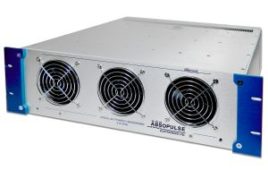
To understand how this works let’s examine the ISL8240MEVAL4Z evaluation board implementation (Figure 2). It’s a four-layer board that supports the step-down power module in its dual output mode sourcing 20 A on each output.
Figure 2: ISL8240MEVAL4Z power module evaluation board
The board uses four PCB layers with a nominal thickness of 0.062 in. (±10%), and it has a stack arrangement as shown in Figure 3.
Figure 3: Stack arrangement of four-layer 0.062-in. board used by ISL8240M power module
The PCB is composed primarily of FR4 circuit board material and copper with smaller amounts of solder, nickel, and gold. Table 1 lists the thermal conductivity factors of the primary materials.
Table 1 Thermal Conductivity Factors for PCB Materials
- SAC305* is the most widely used lead-free solder composed of tin 96.5%, silver 3.0%, and copper 0.5%.
- W = watts, in = inches, C = degrees C, m = meters, K =degrees Kelvin
To determine the thermal resistance of a material we use Equation 1.
Equation 1: Materials thermal resistance calculation
To determine the thermal resistance of the boards top copper layer in Figure 3, take the thickness of the copper layer (t) and divide it by the thermal conductivity factor multiplied by the cross sectional area. We have conveniently used 1 in2 with the dimensions A = B = 1 in. as the cross sectional area. The thickness of the copper layer is 2.8 mil or 0.0028 in. This is the thickness of 2 oz. of copper deposited on 1 ft.2 of board area. The factor K is the W/(in-°C) factor for copper, which is 9. Therefore the thermal resistance to heat flow of this 1 in2 of 2.8-mil copper is 0.0028/9 = 0.0003 °C/W. You can use the dimension shown in Figure 3 for each layer and the appropriate K factor from Table 1 to calculate the thermal resistance of each layer of the one square inch board area. The results are shown in Figure 4.
Figure 4: Thermal resistance of the 1 in2 board layers
From these numbers, we can see that the 33.4 mil (t5) layer has the highest thermal impedance. All the numbers in figure 4 show the total thermal impedance of one square inch of this four layer board from the top layer to the bottom layer. What happens if we add one via connection through the board from top to bottom? Let’s examine adding that via connection.
The board uses vias that have a finished hole size of about 12 mils (0.012 in.). To build the via, the hole is drilled 0.014 in. in diameter and then plated. The plating adds a copper wall to the inside of the hole that is about 1 mil (0.001 in.) thick. This particular board is also plated using an ENIG process. This adds about 200 μin. of nickel and about 5 μin. of gold onto the outer copper surfaces. We will ignore these and just use the copper in our calculations to determine the thermal resistance of the via.
Equation 2 describes the equation for a cylindrical tube.
θ = l / K π (r12 – r02)
Equation 2: Cylindrical tube calculation
Variable l is the length of the cylinder, K is the thermal conductivity factor, r1 is the larger radius and r0 is the smaller radius.
Using this equation for the 12 mil (diameter) finished hole we have r0 = 6 mils (0.006 in), r1 = 7 mils (0.007 in) and K =9 for the copper plating.
Figure 5: Surface dimensions of 12 mil via
Variable l is the length of the via which goes from the top copper layer to the bottom copper layer. There will be no solder mask where the module is soldered to the board, but for other areas, the PCB designer may request that the solder mask be placed on top of each via or the area above the via may be voided. Since the via only connects the outer copper layers, its length is 63.4 mils, or 0.0634 inches. The thermal resistance for the total via length by itself is 167 °C/W as shown in Equation 3.
Equation 3: Calculation for thermal resistance of one via (12 mil)
Figure 6 lists the thermal resistance for each via segment that connects the various layers of the board.
Figure 6: Thermal resistances for the via segments connecting each layer
Note that these values are only the thermal resistance of the one via by itself, not considering that each segment laterally connects through the board to the materials around it.
If we examine the thermal resistance values of the board layers in Figure 4 and compare them to the thermal resistance values for one via, it appears that the via has much higher thermal impedance for each layer, but note that one via occupies less than 1/5000th of the square inch of board area.
If we decided to compare a smaller board area, say 0.25× 0.25 in, (this would be 1/16th of the previous board area) the thermal resistance values in Figure 4 would each increase by 16×. For example, the thermal impedance of t4, and the 33.4 mil thick FR4 layer, would increase from 5.21875 to 83.5 °C/W. Adding only one via to this 0.25 × 0.25-in area will reduce the thermal impedance through this 33.4-mil FR4 layer by almost half [83.5 °C/W in parallel with 90.91 °C/W) . The area of the 0.25 × 0.25-in square is about 400 times greater than the area of the one via. So what happens when we place 16 vias in this area? It reduces the effective thermal resistance of all the vias in parallel by 16× when compared to a single via. Figure 7 compares the thermal resistances of the board layers for the 0.25 × 0.25-in segment to that of 16 vias. The 33.4-mil-thick FR4 layer of the 0.25 × 0.25-in board has a thermal impedance of 83.5 °C/W. The 16 parallel vias have an equivalent thermal impedance of 5.6821 °C/W.
These 16 vias will occupy less than 1/25th of the area of the 0.25 × 0.25-in board area but significantly reduce the thermal impedance connections from the top surface to the lower layers.
Figure 7: Thermal resistance values comparison
Note that when the heat flows down a via and hits another layer, especially another copper layer, the heat will move laterally away from the via into that material layer. Adding more and more vias eventually has diminishing returns because the heat moving laterally out of one via into the adjacent material will eventually run into heat coming from another direction that originated from another via.
The ISL8240MEVAL4Z board is 3 ×4 in. The board has 2-oz. copper on top and bottom layers and two internal layers of 2-oz. copper. To make all this copper useful the board has 917 12-mil vias, all of which aid in moving heat out of the module down into the copper layers below.
References:
- For more information about the ISL8240MEVAL4Z evaluation board: http://www.intersil.com/en/tools/reference-designs/isl8240mevalxz.html
- For more information about the ISL8240M Dual 20A/Single 40A Step-Down Power Module: http://www.intersil.com/products/ISL8240M
About the author:
Jerome Johnston is an Applications Engineer with Intersil Corporation’s Central Applications team. He has more than 30 years of analog system design and applications experience. Jerome received his BSEE from the University of Nebraska and has 13 patents, three in instrumentation, and ten in silicon design of A/D converters.
Filed Under: Power Electronic Tips