The scanning electron microscope (SEM) is capable of imaging an object with a resolution of better than one nanometer. To put that in perspective, a meter is to the size of the earth as a nanometer is to the size of a marble. A nanometer, at the small limit of nanotechnology by definition, is a billionth (10-9) of a meter. A hydrogen atom is one-quarter of a nanometer in diameter. A bacterium is 0.5 to 5 micrometers long, orders of magnitude larger.
The scanning electron microscope is capable or rendering images at magnifications ranging from 10X to 500,000X, 250 times the limit of the most powerful optical microscopes.
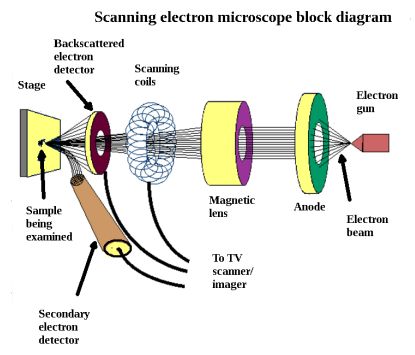
A SEM produces a beam of electrons with an electron gun. The electron beam follows a path through the microscope within a vacuum, through electromagnetic fields and lenses, which focus it down toward the sample. Once the beam hits the sample, electrons and X-rays are ejected from the sample. Detectors collect these X-rays, backscattered electrons, and secondary electrons and convert them into a signal that goes to a screen similar to a television screen. This produces the final image.
The SEM images a sample by scanning it with a highly focused beam of electrons. Striking individual atoms in the sample under investigation, the electrons are subsequently detected, whereupon it is possible to extract information regarding surface details as well as inner structure.
Objects of interest may be observed at close to 0°K, or at elevated temperatures, wet or dry, and pressurized or in a vacuum.
The first true SEMs were built in the 1930s, but they did not become commercially available for another 30 years. Currently, a number of manufacturers produce these complex instruments. They are expensive. Generally, prices are not even quoted on vendor websites.
As might be expected, the process of scanning with a concentrated beam of electrons could create a strong electrostatic charge that would prevent imaging. For this reason, it is necessary to connect the sample to electrical ground. If the sample is metallic, this does not present a problem, but nonmetallic objects must be prepared through the application of a plating (specifically, sputtering, not conventional electroplating) prior to imaging. Gold is frequently used. Another approach is to restrict the scanning to a low-voltage mode.
SEMs are widely used in the analysis of integrated circuits, where challenging size frontiers are encountered.
SEM operation is generally based on thermionic emission from an electron gun that has a tungsten filament cathode. Tungsten is suitable because it has a high melting point and low vapor pressure.
Condenser lenses and scanning coils or deflector plates focus the 0.2 keV to 40 keV electron beam onto the sample, covering an area under 5 nm in diameter.
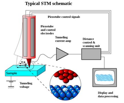
The scanning tunneling microscope (STM) differs significantly from the SEM. It is capable of imaging objects at ten times the lateral resolution, to 0.1 nanometer. This is well down into the quantum realm. Quantum mechanics is the theoretical basis for tunneling. From a classical perspective, if a conventional object encounters an impenetrable barrier, it will go no farther. In the quantum domain, however, an object with minimal mass, for example an electron, also possesses the attributes of a wave, which enable it to cross the otherwise impenetrable barrier. This activity is known as tunneling. It arises when electrons are at or near the Fermi level.
An STM at the London Centre for Nanotechnology.
The central concept in the STM is that of a small conducting tip brought near to the sample. A bias voltage is applied between these two points and electrons proceed to cross the vacuum between them. The amount of tunneling current — which in accordance with Kirchhoff’s Current Law can be measured at any point in the circuit — depends upon tip position, applied voltage and local density state of the sample. Because the first two of these variables are known, the third can be readily calculated as the scanning proceeds, and this provides the basis for the imaging.
Change in current with respect to position or change in position with respect to current can be mapped. These two methodologies are known as constant height mode and constant current mode.
 As may be expected, imaging at the high resolutions the STM can produce will not be possible if there is any vibration at all, so isolation and a rigid frame are essential just to get started. Magnetic levitation has been used in the past, but at present the usual strategy is mechanical or gas spring mounting.
In addition to imaging, the STM tip is used to actually manipulate objects on an atomic scale. There is great debate over where this will all go. Because STM equipment is on the cutting edge of technology, it has become a focus of interest. Proponents of nanotechnology are enthusiastic while the doomsday community see a downside.
Gray goo is a term that is used to describe an end-of-world catastrophic event in which self-replicating micro-robots consume the entire earth seeking material to build more of themselves. A History Channel broadcast speculated that self-replicating nano-robots could be released off the coast of Louisiana to clean up an oil spill. Because of a programming error, they might not restrict their diet to off-shore petroleum products, instead looking inland for nourishment. “Within days the planet is turned to dust,” it speculated under this scenario.
While such a situation appears fanciful, it should remind us that nanotechnology could negatively impact our world. The STM, in this context, could function in ways that at present we are not able to predict.
The post Difference between the scanning electron microscope
and scanning tunneling microscope appeared first on Test & Measurement Tips.
Filed Under: Test & Measurement Tips