Design World

  • Home
  • Technologies
    • 3D CAD
    • Electronics • electrical
    • Fastening & Joining
    • Factory automation
    • Linear Motion
    • Motion Control
    • Test & Measurement
    • Sensors
    • Fluid power
  • Learn
    • Ebooks / Tech Tips
    • Engineering Week
    • Future of Design Engineering
    • MC² Motion Control Classrooms
    • Podcasts
    • Videos
    • Webinars
  • LEAP AWARDS
  • Leadership
    • 2022 Voting
    • 2021 Winners
  • Design Guide Library
  • Resources
    • 3D Cad Models
      • PARTsolutions
      • TraceParts
    • Digital Issues
      • Design World
      • EE World
    • Women in Engineering
  • Supplier Listings

45nm and Beyond

By Design World Staff | November 29, 2007

Share

Applied Materials, Inc. today announced its new Applied FullVision™ system that enables real-time control of dielectric CMP1 processes to the 45 nanometer (nm) device node and beyond. The FullVision system couples Applied’s patented window-in-pad technology with multiple-wavelength spectroscopy to deliver advanced in situ endpoint capability for a variety of dielectric materials, including oxide, STI2, and poly CMP applications. The system demonstrates high repeatability across all applications with less than 150 angstrom, 3-sigma endpoint accuracy on patterned wafers. A major advance over single wavelength endpoint technologies, the FullVision system offers improved measurement accuracy with 50% higher reliability for dielectric applications.

“CMP endpoint technology was pioneered by Applied Materials and is key to delivering benchmark CMP performance,” said Dr. Hichem M’Saad, vice president and general manager of Applied Materials’ Dielectric Systems and CMP Business Group. “As films become thinner, CMP becomes increasingly difficult, requiring much more precise wafer-to-wafer process control to achieve acceptable yields. Using broadband spectral analysis, FullVision technology monitors individual polishing zones across the wafer to provide twice the accuracy and repeatability of competitive systems on a wide variety of process steps — without compromising throughput. These are vital requirements for advanced device manufacturing.”

The FullVision system has already been adopted by major memory customers on their Applied Reflexion® LK CMP systems in high volume manufacturing. For these customers, the system has enabled higher CMP yield by significantly reducing wafer scrap caused by drifts in consumable sets and incoming wafer profile variations.
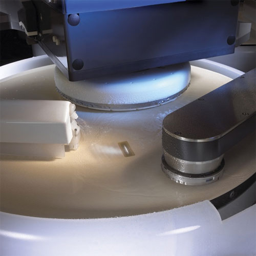
amat-cmp.jpg

The Applied FullVision CMP endpoint system is a major advancement over single wavelength endpoint technologies, offering twice the measurement accuracy with 50% higher reliability for dielectric applications, including oxide, STI and poly CMP.

Applied Materials leads the industry in CMP technology – with an installed base of more than 900 300mm CMP systems worldwide – and in providing advanced in situ metrology for ensuring best-of-breed planarization performance. See http://appliedmaterials.com/products/reflexion_lk_cmp_4.html for more information on the Applied FullVision endpoint system.

www.appliedmaterials.com

1 CMP=chemical mechanical planarization

2 STI=shallow trench isolation


Filed Under: Semiconductor, Materials • advanced


Tell Us What You Think!

Related Articles Read More >

Self-lubricating and wear-resistant: igus bar stock for food, continuous operation and high media resistance
Minnesota Rubber and Plastics announces plans for new Innovation Center
The importance of resin selection
EXE014 - Image 1
Composite materials help place Italian race team in pole position

DESIGN GUIDE LIBRARY

“motion

Enews Sign Up

Motion Control Classroom

Design World Digital Edition

cover

Browse the most current issue of Design World and back issues in an easy to use high quality format. Clip, share and download with the leading design engineering magazine today.

EDABoard the Forum for Electronics

Top global problem solving EE forum covering Microcontrollers, DSP, Networking, Analog and Digital Design, RF, Power Electronics, PCB Routing and much more

EDABoard: Forum for electronics

Sponsored Content

  • Global supply needs drive increased manufacturing footprint development
  • How to Increase Rotational Capacity for a Retaining Ring
  • Cordis high resolution electronic proportional pressure controls
  • WAGO’s custom designed interface wiring system making industrial applications easier
  • 10 Reasons to Specify Valve Manifolds
  • Case study: How a 3D-printed tool saved thousands of hours and dollars

Design World Podcasts

May 17, 2022
Another view on additive and the aerospace industry
See More >
Engineering Exchange

The Engineering Exchange is a global educational networking community for engineers.

Connect, share, and learn today »

Design World
  • Advertising
  • About us
  • Contact
  • Manage your Design World Subscription
  • Subscribe
  • Design World Digital Network
  • Engineering White Papers
  • LEAP AWARDS

Copyright © 2022 WTWH Media LLC. All Rights Reserved. The material on this site may not be reproduced, distributed, transmitted, cached or otherwise used, except with the prior written permission of WTWH Media
Privacy Policy | Advertising | About Us

Search Design World

  • Home
  • Technologies
    • 3D CAD
    • Electronics • electrical
    • Fastening & Joining
    • Factory automation
    • Linear Motion
    • Motion Control
    • Test & Measurement
    • Sensors
    • Fluid power
  • Learn
    • Ebooks / Tech Tips
    • Engineering Week
    • Future of Design Engineering
    • MC² Motion Control Classrooms
    • Podcasts
    • Videos
    • Webinars
  • LEAP AWARDS
  • Leadership
    • 2022 Voting
    • 2021 Winners
  • Design Guide Library
  • Resources
    • 3D Cad Models
      • PARTsolutions
      • TraceParts
    • Digital Issues
      • Design World
      • EE World
    • Women in Engineering
  • Supplier Listings