The Copper-Indium-Gallium-Selenium (CIGS) process is arguably the best recipe currently available for thin-film solar cells. Promising efficiencies on par with crystalline silicon and a cost to manufacture that is significantly less (notwithstanding the current commodity price of silicon wafers from China), CIGS research and production is continuing at an accelerated pace.
The production effort is split between the co-deposition process, where the four CIGS components are simultaneously vaporized onto the substrate in a vacuum system, and the CIG + Se “furnace process,” where a sputtered CIG layer is exposed to selenium vapor, which is then driven into the film in a rapid thermal process step. Both methods have yielded cells with efficiencies of more than 20% in laboratory tests, and both have yielded cells of less than half that in production operations.
The discrepancy between the “Lab to Fab” numbers can be traced, in part, to the process control systems used in the cell manufacture. It’s one thing to carefully control a research level chamber using state of the art film thickness measurement tools, where Angstrom level accuracy and controlled conditions prevail. It’s quite another to monitor a continuous production line where the movement of substrates and materials wreaks havoc on even the most robust measurement scheme.

A critical metric for CIGS films is the absolute thickness of the individual component or compound layers. The ratio of each material in the final product determines in large part the efficiency of the finished cell. Using vacuum or atmospheric pressure deposition, the mixing ratios of the elements can be determined by measuring the rate, in Angstroms or nanometers, per second. There are few instruments that can do this real time, however. One is an optical method called emission spectroscopy, while the other is mass based. The latter is referred to as a quartz crystal microbalance, or QCM for short.
Emission systems work well when calibrated properly but have the tendency to “drift” or fall out of calibration over time. The QCM, on the other hand, is extremely accurate but suffers from a limited life of the quartz crystal used in continuous production. Further, one of the components in CIGS, selenium, is a high vapor pressure material that can infiltrate the housing holding the crystal sensor, leading to short-circuiting and ultimately failure. As a result, QCM’s have severe limitations in CIGS lines that must be addressed by work-arounds.
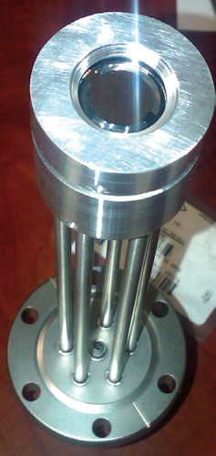
A new generation QCM has been developed that addresses these selenium issues and solves the “drift” problem of emission spectroscopy. This QCM, the Colnatec Helios, features two innovations:
1) a self-cleaning mechanism that allows the quartz sensor to be heated past the selenium evaporation temperature, causing the film to “re-evaporate” off the surface (effectively bringing the crystal to like-new” condition after it has reached its useful life); and
2) a high temperature (300° C) sealing mechanism that prevents the selenium vapor from penetrating the housing used to hold the crystal.
Helios offers the same Angstrom level accuracy as traditional QCMs but without the limitations. Further, using an advanced-regulation system employed in the electronics that mates to the Helios, there is no variation in absolute calibration of the sensor.
This surpasses the emission spectroscopic method in ultimate measurement accuracy and does so at a significantly reduced cost. The Helios system can also be calibrated to match thickness standards, meaning the “Lab to Fab” errors are significantly reduced. Helios can operate in vacuum, atmosphere or even overpressure systems.
Scott Grimshaw
CTO, ColnaTec
Editorial Director
ColnaTec
www.colnatec.com
::Design World::
Filed Under: Green engineering • renewable energy • sustainability, Materials • advanced


Tell Us What You Think!