Image Credit: AGC Asahi Glass
AGC Asahi Glass, a Tokyo glass manufacturer, will release a line of glass substrates designed for semiconductor packaging at NEPCON JAPAN 2017. The conference kicks off today in Tokyo and runs through Friday.
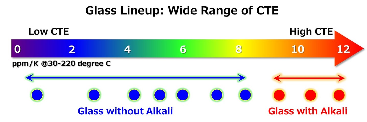
The need for glass wafers, AGC says, sprung up from the development of wafer-level packaging technology in which the integrated circuit is packaged while still part of the wafer. This technology has led to progress with next-generation semiconductor and MEMS devices. These new glass wafers can match silicon’s coefficient of thermal expansion, eliminating the warping that occurs when attempting to directly laminate silicon and glass wafers whose CTE values differ.
The new glass substrates are available in rectangular and square shapes, as well as traditional round wafers with thicknesses ranging from 0.2 mm to 2 mm. The product lines the company will unveil at NEPCON JAPAN include glass without alkali, which maintain the exact same CTE as silicon through temperatures up to 250° Celsius, as well as glass with alkali, covering higher ranges up to CTE 12 ppm/°C.
You can learn more about NEPCON JAPAN 2017 here.
Filed Under: Rapid prototyping