Design World

  • Home
  • Technologies
    • 3D CAD
    • Electronics • electrical
    • Fastening & Joining
    • Factory automation
    • Linear Motion
    • Motion Control
    • Test & Measurement
    • Sensors
    • Fluid power
  • Learn
    • Ebooks / Tech Tips
    • Engineering Week
    • Future of Design Engineering
    • MC² Motion Control Classrooms
    • Podcasts
    • Videos
    • Webinars
  • LEAP AWARDS
  • Leadership
    • 2022 Voting
    • 2021 Winners
  • Design Guide Library
  • Resources
    • Subscribe!
    • 3D Cad Models
      • PARTsolutions
      • TraceParts
    • Digital Issues
      • Design World
      • EE World
    • Women in Engineering
  • Supplier Listings

Applied Aera2™ for Lithography from Applied Materials

By Design World Staff | December 1, 2008

Share


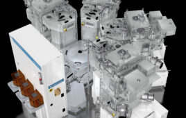
SANTA CLARA, Calif.–Applied Materials, Inc. announces its Applied Aera2‚â„¢ for Lithography system. Using the system‚’s IntenCD‚â„¢ technology in the fab, semiconductor manufacturers can improve wafer critical dimension uniformity (CDU) by more than 20%, increasing device yield and lowering the per-wafer cost of patterning. In addition, the Aera2 for Lithography can be used to extend photomask lifetime and bring productivity gains to the entire lithography cell.

applied-aera2.jpg


Key to this new lithography application is the Aera2 platform‚’s IntenCD technology that creates high precision, high definition CDU maps from the aerial image of an entire reticle. By replacing wafer-based measurements with IntenCD maps, the time to decision shrinks from two days to as little as an hour, and accuracy improves by eliminating cumulative errors that can arise from multiple wafer processing steps. The improved uniformity data allows advanced scanners to compensate for CD variations, delivering major improvements in linewidth accuracy on product wafers and ultimately, increased yield.


Regularly inspecting masks within the fab using the IntenCD technology can stretch photomask lifetime significantly, a compelling benefit in an era when a single mask for a critical device layer can cost more than $100,000. Mask properties change dynamically and non-uniformly with cumulative exposure, inducing CD errors from haze defect growth and pellicle degradation. By replacing traditional fixed mask reconditioning intervals with predictive scheduling, fab managers can use the Aera2 system to minimize mask reconditioning cycles, increasing mask lifetime and availability.


To optimize cycle time, the industry-leading Applied Tetra‚â„¢ Reticle Clean system can also be added to the lithography cell, eliminating the need to send masks outside the fab for reconditioning. The Aera2 for Lithography and the Tetra Reticle Clean are Applied‚’s most recent additions to its strong, proven line-up of solutions to enable cost-effective patterning of next-generation devices.


www.appliedmaterials.com/products/mask_inspection_4.html


::Design World::


Filed Under: Semiconductor


Tell Us What You Think!

Related Articles Read More >

sager electronics
Sager Electronics adds electronic CAD file accessibility in online catalog
Samsung Foundry certifies analog FastSPICE platform from Siemens for early design starts on 3nm GAA process technology
richardson
Richardson Electronics to offer Fuji Electric 7th-generation (X-Series) IGBT modules
How to get the most from flash storage

DESIGN GUIDE LIBRARY

“motion

Enews Sign Up

Motion Control Classroom

Design World Digital Edition

cover

Browse the most current issue of Design World and back issues in an easy to use high quality format. Clip, share and download with the leading design engineering magazine today.

EDABoard the Forum for Electronics

Top global problem solving EE forum covering Microcontrollers, DSP, Networking, Analog and Digital Design, RF, Power Electronics, PCB Routing and much more

EDABoard: Forum for electronics

Sponsored Content

  • Industrial disc pack couplings
  • Pushing performance: Adding functionality to terminal blocks
  • Get to Know Würth Industrial Division
  • Renishaw next-generation FORTiS™ enclosed linear encoders offer enhanced metrology and reliability for machine tools
  • WAGO’s smartDESIGNER Online Provides Seamless Progression for Projects
  • Epoxy Certified for UL 1203 Standard

Design World Podcasts

July 26, 2022
Tech Tuesdays: Sorbothane marks 40 years of shock and vibration innovation
See More >
Engineering Exchange

The Engineering Exchange is a global educational networking community for engineers.

Connect, share, and learn today »

Design World
  • Advertising
  • About us
  • Contact
  • Manage your Design World Subscription
  • Subscribe
  • Design World Digital Network
  • Engineering White Papers
  • LEAP AWARDS

Copyright © 2022 WTWH Media LLC. All Rights Reserved. The material on this site may not be reproduced, distributed, transmitted, cached or otherwise used, except with the prior written permission of WTWH Media
Privacy Policy | Advertising | About Us

Search Design World

  • Home
  • Technologies
    • 3D CAD
    • Electronics • electrical
    • Fastening & Joining
    • Factory automation
    • Linear Motion
    • Motion Control
    • Test & Measurement
    • Sensors
    • Fluid power
  • Learn
    • Ebooks / Tech Tips
    • Engineering Week
    • Future of Design Engineering
    • MC² Motion Control Classrooms
    • Podcasts
    • Videos
    • Webinars
  • LEAP AWARDS
  • Leadership
    • 2022 Voting
    • 2021 Winners
  • Design Guide Library
  • Resources
    • Subscribe!
    • 3D Cad Models
      • PARTsolutions
      • TraceParts
    • Digital Issues
      • Design World
      • EE World
    • Women in Engineering
  • Supplier Listings