Design World

  • Home
  • Technologies
    • 3D CAD
    • Electronics • electrical
    • Fastening & Joining
    • Factory automation
    • Linear Motion
    • Motion Control
    • Test & Measurement
    • Sensors
    • Fluid power
  • Learn
    • Ebooks / Tech Tips
    • Engineering Week
    • Future of Design Engineering
    • MC² Motion Control Classrooms
    • Podcasts
    • Videos
    • Webinars
  • LEAP AWARDS
  • Leadership
    • 2022 Voting
    • 2021 Winners
  • Design Guide Library
  • Resources
    • 3D Cad Models
      • PARTsolutions
      • TraceParts
    • Digital Issues
      • Design World
      • EE World
    • Women in Engineering
  • Supplier Listings

Applied Materials Inflexion™ Edge Polishing System

By Design World Staff | May 7, 2008

Share


SANTA CLARA, Calif.–Applied Materials, Inc.
(NASDAQ:AMAT) launched its Applied Inflexion™ edge polishing system, a unique, high-precision defect removal system that polishes and cleans the critical wafer edge region. The Applied Inflexion is the only system that polishes the entire wafer edge, removing film stack residues and shallow surface defects in a single pass while minimizing the exclusion area in order to maximize the number of good die. In addition, the system precisely controls the edge profile, enabling customers to tailor the film-to-wafer interface to meet a wide range of integration requirements.
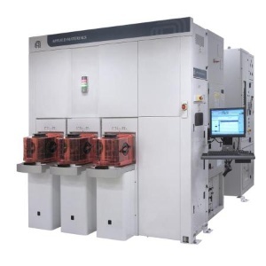
applied materials inflexion.jpg


The Applied Inflexion system’s high productivity platform can be configured with up to three processing modules to deliver twice the throughput of competing edge polishing systems. The system integrates Applied’s production-proven Desica® single wafer wet cleaner to assure excellent defect performance on all surfaces. Using abrasive tape with proprietary head technology, the Inflexion system delivers a non-selective process that efficiently removes all materials, including metal/dielectric stack residues not easily removed by other cleaning methods, from the entire edge region that comprises the notch, bevel, apex, and front and back exclusion zones. For more information, please visit www.appliedmaterials.com/products/edge_polishing_4.html.


When the Applied Inflexion system is used in conjunction with the Applied SEMVision™ G4 defect review tool, these systems provide a comprehensive wafer edge defect removal, review and analysis solution, enabling customers to successfully characterize and control edge defect issues, especially in immersion lithography.


www.appliedmaterials.com

::Design World::


Filed Under: Semiconductor, Materials • advanced


Tell Us What You Think!

Related Articles Read More >

Self-lubricating and wear-resistant: igus bar stock for food, continuous operation and high media resistance
Minnesota Rubber and Plastics announces plans for new Innovation Center
The importance of resin selection
EXE014 - Image 1
Composite materials help place Italian race team in pole position

DESIGN GUIDE LIBRARY

“motion

Enews Sign Up

Motion Control Classroom

Design World Digital Edition

cover

Browse the most current issue of Design World and back issues in an easy to use high quality format. Clip, share and download with the leading design engineering magazine today.

EDABoard the Forum for Electronics

Top global problem solving EE forum covering Microcontrollers, DSP, Networking, Analog and Digital Design, RF, Power Electronics, PCB Routing and much more

EDABoard: Forum for electronics

Sponsored Content

  • Renishaw next-generation FORTiS™ enclosed linear encoders offer enhanced metrology and reliability for machine tools
  • WAGO’s smartDESIGNER Online Provides Seamless Progression for Projects
  • Epoxy Certified for UL 1203 Standard
  • The Importance of Industrial Cable Resistance to Chemicals and Oils
  • Optimize, streamline and increase production capacity with pallet-handling conveyor systems
  • Global supply needs drive increased manufacturing footprint development

Design World Podcasts

June 12, 2022
How to avoid over engineering a part
See More >
Engineering Exchange

The Engineering Exchange is a global educational networking community for engineers.

Connect, share, and learn today »

Design World
  • Advertising
  • About us
  • Contact
  • Manage your Design World Subscription
  • Subscribe
  • Design World Digital Network
  • Engineering White Papers
  • LEAP AWARDS

Copyright © 2022 WTWH Media LLC. All Rights Reserved. The material on this site may not be reproduced, distributed, transmitted, cached or otherwise used, except with the prior written permission of WTWH Media
Privacy Policy | Advertising | About Us

Search Design World

  • Home
  • Technologies
    • 3D CAD
    • Electronics • electrical
    • Fastening & Joining
    • Factory automation
    • Linear Motion
    • Motion Control
    • Test & Measurement
    • Sensors
    • Fluid power
  • Learn
    • Ebooks / Tech Tips
    • Engineering Week
    • Future of Design Engineering
    • MC² Motion Control Classrooms
    • Podcasts
    • Videos
    • Webinars
  • LEAP AWARDS
  • Leadership
    • 2022 Voting
    • 2021 Winners
  • Design Guide Library
  • Resources
    • 3D Cad Models
      • PARTsolutions
      • TraceParts
    • Digital Issues
      • Design World
      • EE World
    • Women in Engineering
  • Supplier Listings