Design World

  • Home
  • Technologies
    • 3D CAD
    • Electronics • electrical
    • Fastening & Joining
    • Factory automation
    • Linear Motion
    • Motion Control
    • Test & Measurement
    • Sensors
    • Fluid power
  • Learn
    • Ebooks / Tech Tips
    • Engineering Week
    • Future of Design Engineering
    • MC² Motion Control Classrooms
    • Podcasts
    • Videos
    • Webinars
  • LEAP AWARDS
  • Leadership
    • 2022 Voting
    • 2021 Winners
  • Design Guide Library
  • Resources
    • 3D Cad Models
      • PARTsolutions
      • TraceParts
    • Digital Issues
      • Design World
      • EE World
    • Women in Engineering
  • Supplier Listings

Applied Materials Ships 250th Vantage System

By Design World Staff | March 29, 2007

Share

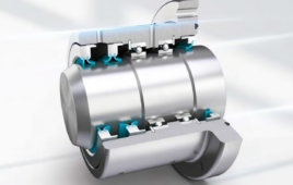
SANTA CLARA, Calif.–(BUSINESS WIRE)–Applied Materials, Inc. announces the shipment of its 250th Applied Vantage® RTP system, the rapid thermal processing (RTP) production system selected by every 300mm device manufacturer worldwide. The system’s innovative design has made it the most productive RTP system in the industry, achieving >90% availability and an unmatched mechanical throughput of >95 wafers per hour in a highly compact footprint. The Vantage’s chambers feature an optimized honeycomb lamp head for maximum heating efficiency and unique multi-point temperature sampling and control technology that ensures superior within-wafer and wafer-to-wafer uniformity.

Radiance_chambers.jpg

“We thank our customers for working with us over the years in our drive to deliver best-in-class RTP performance,” said Tom St. Dennis, senior vice president and general manager of Applied Materials’ Etch, Cleans, Front End and Implant Groups. “As the next generation’s advanced transistors and memory cells require more tightly controlled thermal processing, customers can continue to rely on Applied Materials for advanced RTP technology to meet their most demanding manufacturing challenges.”

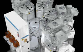
The Applied Vantage is the most flexible thermal processing platform on the market, addressing all spike, soak, contact and silicide anneals, thermal nitridation, and both dry and radical oxidation. Available with the Applied RadiancePlus RTP or Applied RadOx RTP chambers, the system links two process chambers to an Applied factory interface and track robot to maximize productivity per square foot. The entire system ships as one integrated unit, reducing fab install time to =10 days. Learn more about the Applied Vantage RTP system at www.appliedmaterials.com/vantagemilestone.

Applied Materials has more than 2,400 RTP chambers installed worldwide on its Vantage and Centura® platforms. According to VLSI Research, the RTP market is expected to grow at a compound annual rate of 12% from 2006-2011.

Applied Materials, Inc. (Nasdaq:AMAT) is the global leader in Nanomanufacturing Technology™ with a broad portfolio of innovative equipment, service and software products for the fabrication of semiconductor chips, flat panels, solar photovoltaic cells, flexible electronics and energy efficient glass. At Applied Materials, we apply Nanomanufacturing Technology to improve the way people live. Learn more at www.appliedmaterials.com.


Filed Under: Semiconductor


Tell Us What You Think!

Related Articles Read More >

sager electronics
Sager Electronics adds electronic CAD file accessibility in online catalog
Samsung Foundry certifies analog FastSPICE platform from Siemens for early design starts on 3nm GAA process technology
richardson
Richardson Electronics to offer Fuji Electric 7th-generation (X-Series) IGBT modules
How to get the most from flash storage

DESIGN GUIDE LIBRARY

“motion

Enews Sign Up

Motion Control Classroom

Design World Digital Edition

cover

Browse the most current issue of Design World and back issues in an easy to use high quality format. Clip, share and download with the leading design engineering magazine today.

EDABoard the Forum for Electronics

Top global problem solving EE forum covering Microcontrollers, DSP, Networking, Analog and Digital Design, RF, Power Electronics, PCB Routing and much more

EDABoard: Forum for electronics

Sponsored Content

  • Renishaw next-generation FORTiS™ enclosed linear encoders offer enhanced metrology and reliability for machine tools
  • WAGO’s smartDESIGNER Online Provides Seamless Progression for Projects
  • Epoxy Certified for UL 1203 Standard
  • The Importance of Industrial Cable Resistance to Chemicals and Oils
  • Optimize, streamline and increase production capacity with pallet-handling conveyor systems
  • Global supply needs drive increased manufacturing footprint development

Design World Podcasts

June 12, 2022
How to avoid over engineering a part
See More >
Engineering Exchange

The Engineering Exchange is a global educational networking community for engineers.

Connect, share, and learn today »

Design World
  • Advertising
  • About us
  • Contact
  • Manage your Design World Subscription
  • Subscribe
  • Design World Digital Network
  • Engineering White Papers
  • LEAP AWARDS

Copyright © 2022 WTWH Media LLC. All Rights Reserved. The material on this site may not be reproduced, distributed, transmitted, cached or otherwise used, except with the prior written permission of WTWH Media
Privacy Policy | Advertising | About Us

Search Design World

  • Home
  • Technologies
    • 3D CAD
    • Electronics • electrical
    • Fastening & Joining
    • Factory automation
    • Linear Motion
    • Motion Control
    • Test & Measurement
    • Sensors
    • Fluid power
  • Learn
    • Ebooks / Tech Tips
    • Engineering Week
    • Future of Design Engineering
    • MC² Motion Control Classrooms
    • Podcasts
    • Videos
    • Webinars
  • LEAP AWARDS
  • Leadership
    • 2022 Voting
    • 2021 Winners
  • Design Guide Library
  • Resources
    • 3D Cad Models
      • PARTsolutions
      • TraceParts
    • Digital Issues
      • Design World
      • EE World
    • Women in Engineering
  • Supplier Listings