“The semiconductor industry is going to have to figure out how to supply customers with the chips that make for better cell phones, lighter ultra-mobile PCs, portable multimedia players with pico-projectors, handheld gaming devices, safer automobile sensors, and more sophisticated
medical imaging equipment,” said Dan Donabedian, CEO, Ziptronix Inc., Research Triangle Park, NC. “And they will have to implement 3D IC technology to realize the higher density, lower costs and increased function, connectivity, and reliability that these applications will require.”

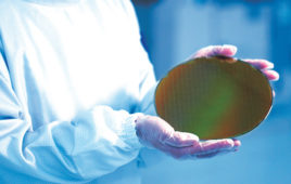
According to Donabedian, one of the crucial elements for successful implementation of 3D IC technology is a reliable, economical, low temperature oxide bonding process that will enable true 3D integration of semiconductors. “A high throughput bonding process that works without requiring high temperature or compression has long been seen as the ‘missing link’ in the 3D IC supply chain,” he explained.
Applications that will benefit from 3D IC technology include:
• Mobile phones with high-resolution digital cameras and increased functions
• Ultramobile, low power, lightweight PCs
• Interactive handheld gaming devices with projection capabilities
• Embedded pico-projectors in a variety of portable multimedia devices
• Advanced automotive sensors (lane change/collision warning)
• Medical imaging systems
Ziptronix 3D
www.ziptronix.com
::Design World::
Filed Under: Semiconductor manufacture


Tell Us What You Think!