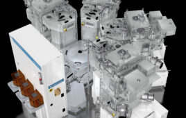
Applied Materials, Inc. and DISCO Corp., announced a joint effort to develop wafer thinning processes for fabricating Through-Silicon Vias (TSVs) in 3D semiconductors. The two companies will work together to develop integrated process flows intended to lower the cost, reduce the risk, and accelerate time to market for next generation chips.

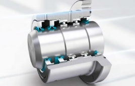
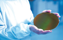
The processes will create higher density, lower-power devices in a smaller footprint by vertically stacking chips. For a 3D stack, each chip or wafer layer must be reduced in thickness by up to 90% and bonded to a temporary carrier to maintain structural integrity during the thermal and mechanical stresses of semiconductor processing.
Combining DISCO‚’s precision grinding equipment with Applied‚’s etch, dielectric deposition, physical vapor deposition and chemical mechanical planarization systems, the two companies expect to develop wafer thinning and post-thinning processes of wafers bonded to silicon and glass carriers. Some of the key technical requirements in developing manufacturing worthy equipment and processes are wafer structural and edge integrity, handling, dimensional control, particle control, stress management and thermal profile control.
DISCO Corp.
www.disco.co.jp
Applied Materials, Inc.
www.appliedmaterials.com
::Design World::
Filed Under: Semiconductor manufacture

Tell Us What You Think!