Design World

  • Home
  • Technologies
    • 3D CAD
    • Electronics • electrical
    • Fastening & Joining
    • Factory automation
    • Linear Motion
    • Motion Control
    • Test & Measurement
    • Sensors
    • Fluid power
  • Learn
    • Ebooks / Tech Tips
    • Engineering Week
    • Future of Design Engineering
    • MC² Motion Control Classrooms
    • Podcasts
    • Videos
    • Webinars
  • LEAP AWARDS
  • Leadership
    • 2022 Voting
    • 2021 Winners
  • Design Guide Library
  • Resources
    • 3D Cad Models
      • PARTsolutions
      • TraceParts
    • Digital Issues
      • Design World
      • EE World
    • Women in Engineering
  • Supplier Listings

Designer Crystals for Next-Gen Electronics

By CSIRO | December 14, 2015

Share

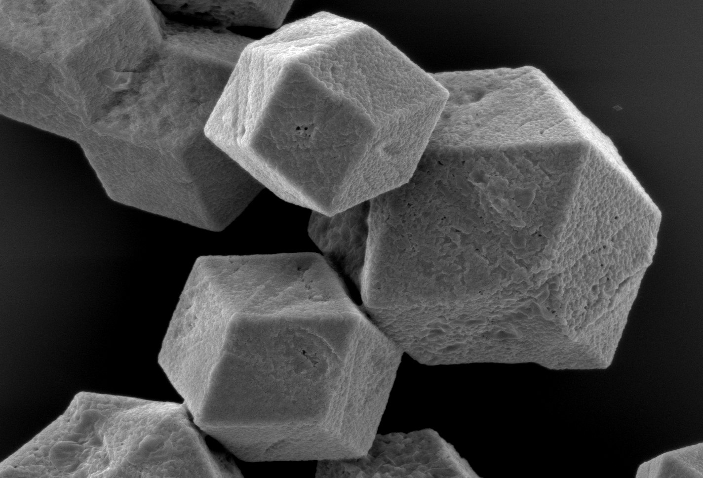
A close up of the metal organic framework crystals. (Credit: CSIRO)

Liquid is often seen as the kryptonite of electronics, known for damaging and corroding components.

That’s why a new process that uses vapour- rather than liquid – to grow designer crystals could lead to a new breed of faster, more powerful electronic devices.

The method, invented by an international team of scientists from the University of Leuven in Belgium, the National University of Singapore and CSIRO has been published today in the journal Nature Materials.

For the first time, the researchers have shown how the designer crystals known as ‘metal organic frameworks’ or MOFs, can be grown using a vapour method that is similar to steam hovering over a pot of hot water.

The crystals are the world’s most porous materials, and if applied to microelectronic devices, could significantly boost their processing power.

However according to CSIRO researcher Mark Styles, up until now these crystals could only be grown and applied using a liquid solvent, making them unsuitable for electronics applications.

“Just like your smart phone doesn’t like being dropped in water, electronic devices don’t like the liquid solvent that’s used to grow MOF crystals,” Dr Styles said.

“It can corrode and damage the delicate circuitry.

“Our new vapour method for growing and applying MOF crystals overcomes this barrier and has the potential to disrupt the microelectronics industry.

“On the atomic scale, MOF crystals look like bird cages that can be tailor-made to be different shapes and sizes.

“They have an extremely large surface area, meaning they can be up to 80 per cent empty inside.

“The net result is a structure where almost every atom is exposed to empty space: one gram of MOF crystals has a surface area of over 5000 square metres – that’s the size of a football field.

“Crucially, we can use this vast space to trap other molecules, which can change the properties of a material.

“In the case of electronics, this means we can fit a lot more transistors on a microchip, making it faster and far more powerful.”

The international team, which was led by Ivo Stassen and Professor Rob Ameloot from the University of Leuven in Belgium, drew on specialist X-ray analysis techniques from CSIRO and the Australian Synchrotron to understand how the vapour process works, and how it can be used to grow the MOF crystals.

According to Dr Styles, the applications for MOFs can only be limited by your imagination.

“Another potential use for this technology would be in portable chemical sensing devices that could be used in hazardous environments such as chemical processing plants and underground mines,” he said.


Filed Under: M2M (machine to machine)


Related Articles Read More >

Part 6: IDE and other software for connectivity and IoT design work
Part 4: Edge computing and gateways proliferate for industrial machinery
Part 3: Trends in Ethernet, PoE, IO-Link, HIPERFACE, and single-cable solutions
Machine Learning for Sensors

DESIGN GUIDE LIBRARY

“motion

Enews Sign Up

Motion Control Classroom

Design World Digital Edition

cover

Browse the most current issue of Design World and back issues in an easy to use high quality format. Clip, share and download with the leading design engineering magazine today.

EDABoard the Forum for Electronics

Top global problem solving EE forum covering Microcontrollers, DSP, Networking, Analog and Digital Design, RF, Power Electronics, PCB Routing and much more

EDABoard: Forum for electronics

Sponsored Content

  • Global supply needs drive increased manufacturing footprint development
  • How to Increase Rotational Capacity for a Retaining Ring
  • Cordis high resolution electronic proportional pressure controls
  • WAGO’s custom designed interface wiring system making industrial applications easier
  • 10 Reasons to Specify Valve Manifolds
  • Case study: How a 3D-printed tool saved thousands of hours and dollars

Design World Podcasts

May 17, 2022
Another view on additive and the aerospace industry
See More >
Engineering Exchange

The Engineering Exchange is a global educational networking community for engineers.

Connect, share, and learn today »

Design World
  • Advertising
  • About us
  • Contact
  • Manage your Design World Subscription
  • Subscribe
  • Design World Digital Network
  • Engineering White Papers
  • LEAP AWARDS

Copyright © 2022 WTWH Media LLC. All Rights Reserved. The material on this site may not be reproduced, distributed, transmitted, cached or otherwise used, except with the prior written permission of WTWH Media
Privacy Policy | Advertising | About Us

Search Design World

  • Home
  • Technologies
    • 3D CAD
    • Electronics • electrical
    • Fastening & Joining
    • Factory automation
    • Linear Motion
    • Motion Control
    • Test & Measurement
    • Sensors
    • Fluid power
  • Learn
    • Ebooks / Tech Tips
    • Engineering Week
    • Future of Design Engineering
    • MC² Motion Control Classrooms
    • Podcasts
    • Videos
    • Webinars
  • LEAP AWARDS
  • Leadership
    • 2022 Voting
    • 2021 Winners
  • Design Guide Library
  • Resources
    • 3D Cad Models
      • PARTsolutions
      • TraceParts
    • Digital Issues
      • Design World
      • EE World
    • Women in Engineering
  • Supplier Listings