The circuit integration in system on chip (SOCs) drives today’s embedded system design where the complex and flexible (programmable and configurable) analog, digital, and processing engines are expected to be in a single chip. This trend has led to the fabrication of complex and advanced analog features in SoCs and MCUs.
These flexible analog fabrics not only enable the configuration of the blocks during the design time but also dynamically reconfigure the block function itself during runtime. These multiple-use analog functions are realized with versatile switched capacitor (SC) networks and analog logic that are built-in in modern SoCs and MCUs. This article talks how various analog functions can be built using switched capacitor networks and their practical use in real applications. This article also talks about theory and application of the switched capacitor analog blocks. The multiple useful function with switched capacitor block includes Delta Sigma modulator, mixer, filter, integrator, summer, subtractor, DAC, programmable gain amplifier, comparator, sample & hold, and more.
Intelligent Analog
The analog circuit ecosystem needs resistors and capacitors along with other analog blocks including op-amps, buffers, comparators, and basic analog logics. As making capacitors is easier and cheaper in an integrated circuitry, techniques have been developed to use switched capacitor to emulate resistors. These switched capacitor architectures control the charge transfer between capacitors with the precise timing of switches (see Figure 1). Built-in clocking/timing control makes the analog function change in real time. Such blocks are sometimes referred to as Universal Analog Blocks (UAB).
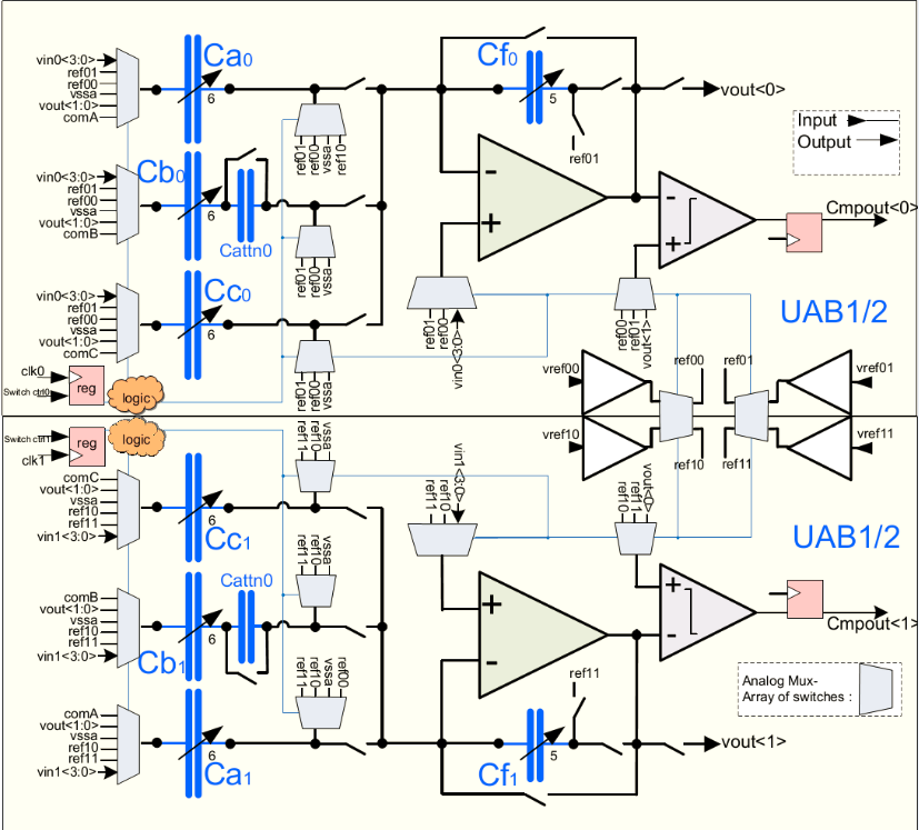
Fig. 1: Universal Analog Block (UAB)
UABs are built with two completely symmetrical half-circuits configurable as either one pseudo-differential or two single-ended functions. Each half circuit comes with control logic for autonomous operation. Figure 2 shows a simplified UAB diagram. UABs have a highly flexible switched and continuous routing fabric to enable complex analog functions like analog filters.

Fig. 2: Simplified UAB Diagram
Theory of charge transfer:
Charge transfer is basically the controlled movement of charge between voltage nodes. Figure 3 shows charge transfer using a resistor and also using a switched capacitor.
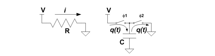
Fig. 3: Simplified UAB Diagram
In the case of a resistor, the current flow (i) is created by the potential difference across the resistance (R). The current is flowing from a voltage potential (V) to ground via the resistor R. This is governed by the following equation:
i = V / R
In the case of a switched capacitor, the current flow (i) is created by charging of capacitance (C) from a higher potential node and discharging it into a lower potential node. When the Φ1 switch is closed and the Φ2 switch is open, the capacitor C charges to the full potential. The charge stored is represented as
q=CV
When the Φ1 switch is opened and the Φ2 switch is closed, all stored charge moves to the ground node. For each switching cycle, a quantum of charge is moved. If the frequency at which the switches are controlled is fs, then the charge quanta also moves at this frequency. The repetitive movement of charge creates a current flow, and it is governed by the equation
i = q/t = fsq = fsCV
Unlike the case with a resistor, current flow is not a continuous movement of charge with a switched capacitor. Comparing the above current equations in both circuits, it is evident that a switched capacitor network is equivalent to a resistor when they have equivalent ratios of voltage drop against delivered current. Thus, we can replace a series resistor with a parallel switched capacitor.
V/i = R = 1/fsC
The equivalent resistor is inversely proportional to the switching frequency and capacitance. The relative value of the resistor may be easily altered by changing the switching frequency. Selecting a larger value of C results in more current and a smaller equivalent resistor. Similarly, driving the switch with a higher frequency (fs) results in a higher current and a lower equivalent resistance. These switches Φ1 and Φ2 have to satisfy the timing requirements to produce the above results. These include:
1) Never close both switches at the same time
2) Give each switch time to open before closing the other switch
3) Select the maximum switched frequency such that the C is fully charged and discharged in the given cycle.
Such a switched capacitor block along with op-amps and comparator form the UAB block. They enable developers to synthesis multiple analog functionalities. One such analog feature, VDAC, is explained in this article.
VDAC Implementation:
VDAC is a digital-to-analog convertor circuit that takes a digital input and converts it into an equivalent analog voltage. At the heart of many control systems, VDACs play a key role in determining system performance ad accuracy. The accuracy of the VDAC output voltage ultimately depends on the accuracy of its reference voltage. There are various applications for VDACs such as using them as a programmable voltage generator to supply sensor bias and offset voltages, comparator reference voltages, or generating dynamic output waveforms.
The UAB switched capacitor topology of a VDAC circuit is shown in the Figure 4. Due the discrete time nature of switched capacitor block, the output is sampled and buffered to get a continuous output. This block is capable of working in both active and sleep mode of the MCU.
This topology gives flexibility to the VDAC functionality. The dynamic Vout range is determined by the Vref value on the one end and Vagnd on the other end. This allows users to set the required dynamic Vout range by providing the Vref and Vagnd from an external circuitry if required. Also, a gain setting allows the output range to be selected as Vagnd+ Vref, Vagnd+ 2Vref or Vagnd+ 4Vref, enabling the complete range between Vssa and Vdda. This VDAC comes with a 13-bit signed input where the input range can be anywhere between -4096 and +4095. These values can be directly written into a corresponding register to take effect.
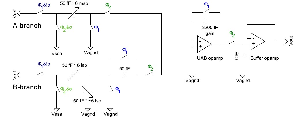
Fig. 4: VDAC based on a switched capacitor topology
VDACs in analog coprocessors also support a multiplying mode wherein the VDAC output voltage is multiplied with an analog input signal to produce a multiplied output. Multiplying DACs (MDAC) are an ideal building block for fixed reference applications where the user wants to generate a waveform from a fixed DC voltage. These MDACs are also suited for various reference applications where the user wants to digitally condition an AC or arbitrary reference voltage.
VDAC IDE configurations:
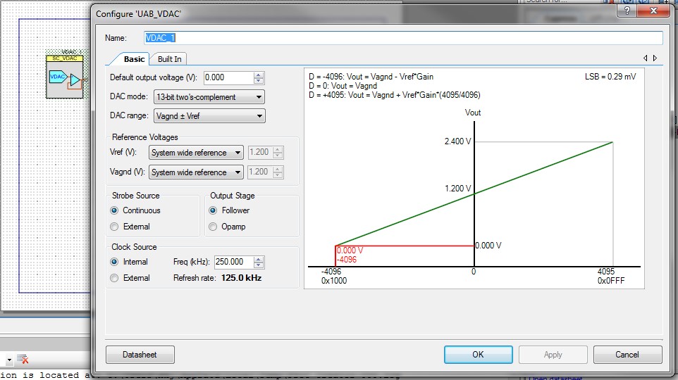
Whenever MCUs provide lot of flexibility and programmability, developers’ worry about configuring lot of registers to tune these blocks for their applications. Analog coprocessor is supported with a tool called to allow easy configurability of these functions. PSoC Creator is a free Windows-based Integrated Development Environment (IDE). It enables concurrent hardware and firmware design systems. This tool is very similar to a lego based design environment wherein a user can place the component on to their schematic just double click the component to configure its features. For example, below figure 4 shows the VDAC component configuration tool in PSoC Creator, Such tools enables faster design cycles.
References:
- AN211293 – Getting Started with PSoC® Analog Coprocessor
- AN86439 – PSoC 4 and PSoC Analog Coprocessor – Using GPIO Pins3. PSoC® Analog Coprocessor
- CY8C4Axx PSoC® Analog Coprocessor Architecture Technical Reference Manual (TRM)
4.PSoC® Analog Coprocessor: CY8C4AXX Family Datasheet
5.CY8CKIT-048 PSoC® Analog Coprocessor Pioneer Kit
Authors:
Jaya Kathuria works as an Applications Manager at Cypress Semiconductor Corporation where she is managing the Embedded Applications Group and Solutions Development using the PSoC platform. She has 11+ years of experience in Semiconductor Industry. She earned executive management credential from IIM, Bangalore and holds BS in Electronics Engineering from the Kurukshetra University. Jaya can be reached at [email protected].
Anbarasu Samiappan is a Senior Applications Manager at Cypress Semiconductor. He is managing PSoC Embedded Systems Group including Customer Technical Support and System validation functions. He is a PMI certified Project Management Professional, Gold medalist Electronics Engineering Graduate from Anna University and earned General Management credential from IIM, Bangalore. He has 19+ years industry experience. Anba can be reached at [email protected].
Filed Under: Capacitors, Materials • advanced