by ADAM BARKLEY, SiC Power Device Application Engineer, Wolfspeed, a Cree Company and VIPINDAS PALA, Research Scientist Wolfspeed, a Cree Company
Engineers increasingly see the logic of silicon-carbide MOSFETs for handling a lot of electrical power, but new SiC devices also make sense for high-voltage switching.
The benefits of silicon-carbide power MOSFETs are becoming widely understood among designers of power electronics. Compared to IGBTs, SiC MOSFETs have a forward characteristic with no knee, which results in higher efficiencies when operating at a low fraction of full power. They also experience five to ten times less switching losses with no current tail during turn-off. Additionally, SiC MOSFETs have an internal body diode with low reverse recovery. These advantages have made SiC MOSFETs a means of realizing higher efficiencies in applications like industrial power supplies, PV inverters and auxiliary power supplies.
Most engineers understand the benefits of SiC MOSFETs compared to IGBTs but are less clear about their superiority over super-junction silicon MOSFETs for devices in the 600-to-900-V class. SiC can enable simpler hard-switched and soft-switched topologies, reduced component counts and simplified over-voltage protection.
A specific case illustrates how SiC MOSFETs can make possible super-efficient and more energy dense power supplies. Researchers devised a single-stage flyback-based LED driver designed around a 900-V, 65 mΩ SiC MOSFET that is part of a recently developed family of devices called C3M. This single-stage flyback topology is widely used in low-power LED drivers (less than 100 W) as often found in tube LED lighting and residential LED lighting. For high-power LED drive applications over 100 W, two-stage topologies, like the boost PFC + LLC half-bridge topology, are preferred because they deliver a more attractive price-performance trade-off when using silicon switches.
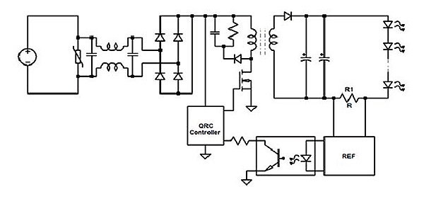
The drawback of single-stage topologies for high-power LED drivers is that the switches see higher voltage and current stresses compared to two-stage topologies. These stresses are exacerbated when wide input and output voltage ranges are required. As a consequence of over-stress when using 650-V-rated switches, single-stage topologies have lower efficiency, narrower operating voltage range, more expensive EMI and surge-protection components, and high output current ripple (flicker).
Extra voltage headroom over 650-V devices makes 900-V silicon MOSFETs potential candidates for the single-stage topology. But 900-V super-junction devices exhibit excessive conduction and switching losses compared to C3M SiC MOSFETs. By combining the required blocking voltage with lower conduction loss, switching loss and device capacitances, C3M 900-V SiC MOSFETs let the single-stage flyback supply operate at higher power density and higher efficiency than the two-stage 650-V topology based on silicon.
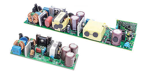
The single-stage LED driver employing SiC MOSFETs takes up 40% less volume and weighs 60% less than existing technology. It is also more efficient than the 650-V silicon two-stage topology and a 900-V silicon MOSFET single-stage topology.
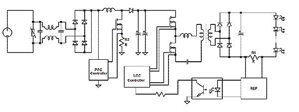
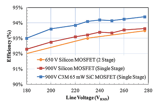
It is interesting to compare a typical high-performance 220-W LED driver using silicon super-junction MOSFETs in a two-stage topology and SiC MOSFETs in a single-stage flyback topology. Both drivers have similar qualities in terms of power, input voltage range, efficiency, THD and power factor. Single-stage topology using an SiC MOSFET is also capable of meeting EMI Class B requirements and surge requirements to 4 kV, L-L while delivering acceptable output current ripple.
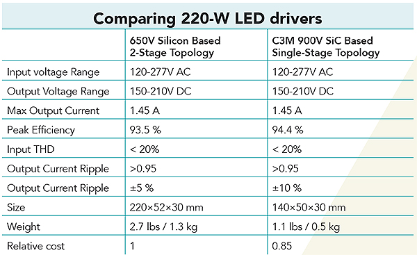
The single-stage design also costs 15% less, mainly through reductions in component count and magnetics. As a result, the cross-over point between single-stage and two-stage topologies rises from 75 to 100 W for silicon LED drivers, to 250 to 300 W for SiC MOSFET drivers.
Improved SiC devices
This compact supply benefits from design improvements in the recently developed SiC MOSFETs dubbed C3M. Compared to earlier SiC MOSFETs, the C3M family of devices has a smaller cell pitch, optimized cell structure and optimized doping levels. The median specific on-resistance of the 900-V SiC MOSFET is 2.3 mΩ·cm2, a 42% reduction over the previous generation.
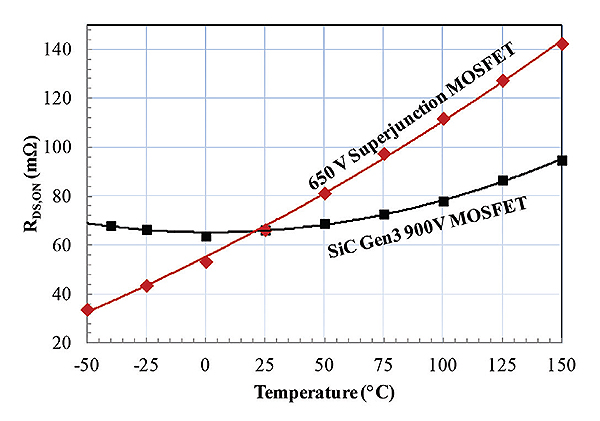
An important feature of 900-V SiC MOSFETs is the low temperature coefficient of on-resistance. On-resistance only rises by 1.4 times between 25 and 150° C. The major reason for this phenomenon is that the MOS channel mobility, which limits on-resistance in SiC MOSFETs, rises at higher temperatures. This effect partially compensates for the rise in drift resistance at high temperatures, thereby reducing the overall temperature coefficient of the device.
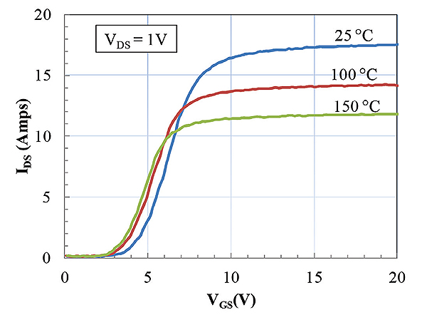
The C3M generation of SiC MOSFETs also has improved transconductance, realized by engineering the MOSFET top-cell structure. The device hits full turn-on at VGS = 15 V at 25° C. Transconductance is even better at 150° C, due to the improvement in channel mobility, so the device fully turns on even at 12 V. In power supply applications, this eases drive requirements compared to previous generations of SiC MOSFETs that needed 18-to-20-V gate bias for full turn-on.
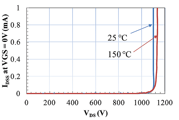
The typical avalanche voltage is 1,100 V at 25° C and 1,130 V at 150° C. Improvements in material quality and optimization of device structure have reduced internal fields in the transistor, which has resulted in extremely stable behavior at high temperature reverse bias (HTRB) conditions.
When stressed at accelerated voltages close to breakdown (> 1 kV) at a junction temperature greater than 150° C, no device failures have been observed even after nine million device-hours. This indicates that C3M devices don’t see the typical failure modes, like gate oxide rupture, observed in earlier-generation SiC MOSFETs under accelerated HTRB conditions.
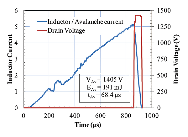
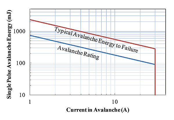
C3M 900-V MOSFETs also show extremely stable avalanche behavior. They’ve been fully qualified for avalanche current withstand capability under unclamped inductive switching (UIS). The avalanche voltage at high currents can be as high as 1.4 kV. The high avalanche voltage observed during UIS arises from the high internal device temperatures (close to 600° C) reached during the UIS event. It is impressive that SiC devices still function after such an extreme event.
Aside from driving lower semiconductor costs, low specific on-resistance of the C3M SiC MOSFET technology can lead to improved dynamic performance for two reasons. First, the smaller chip size reduces internal device capacitances. Consequently, there’s a reduction in switching losses for the same absolute on-resistance. Second, a smaller chip size fits in a smaller form-factor package for the same on-resistance, so the parasitic impedances outside the chip can be minimized.
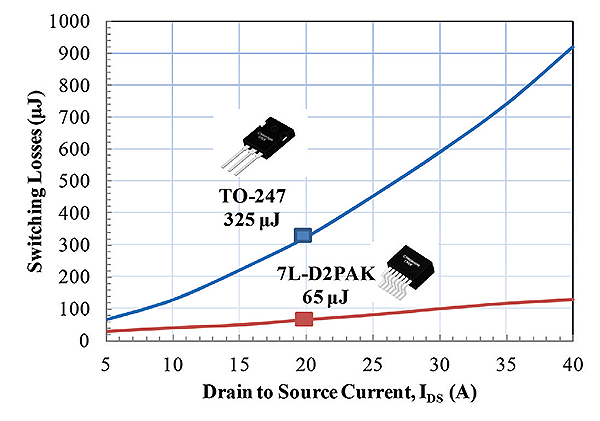
In hard-switched applications, the turn-on and turn-off energy losses for the C3M SiC MOSFET are influenced by the package to a large degree. Consider the switching losses of the C3M 900-V, 65 mΩ MOSFET chip in a TO-247 three-lead package versus those of a seven-lead D2PAK surface mount package with a Kelvin source connection. In one case, the chip has a 5-times-lower switching loss in a 7L-D2PAK compared to the TO-247. This is primarily because of the Kelvin source connection in the 7L-D2PAK, which reduces the gate de-biasing that can arise from the voltage drop across the parasitic source inductance in the package.
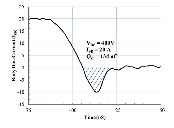
C3M 900-V MOSFETs also have a rugged body diode. Improvements in material and process quality have resulted in the elimination of body diode degradation in SiC MOSFETs. Body diode reverse recovery for the C3M MOSFET is also extremely low. A low recovery body diode lets the device work in half-bridge topologies and in other applications where third-quadrant performance is important.
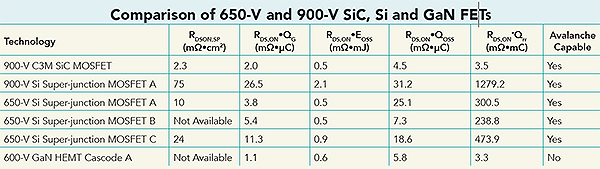
The specific on-resistance of C3M MOSFETs is approximately 30 times smaller than that of conventional 900-V silicon MOSFETs and four times smaller than the state-of-the-art, 650-V, super-junction MOSFETs. The low on-resistance gives the 900-V SiC MOSFET a big advantage over competing technologies in terms of switching performance.
In addition, it is noteworthy that at a junction temperature of 150° C, the on-resistance of silicon and GaN devices rise by a factor of 2 to 2.4 times, whereas the on-resistance of the SiC MOSFET increases only by a factor of 1.4. In hard-switched topologies, switching losses are determined by on-off transition times of the switch, which depends on the gate drive. The figure of merit (FOM) that determines the transition time for a certain gate drive current is RDS,ON•QG. C3M SiC MOSFETs have 13 times lower gate-charge than 900-V silicon MOSFETs and 1.9 times lower than best-in-class, 650-V silicon MOSFETs.
In practice, gate drive speeds are limited by external gate resistors, which are needed to control oscillations that arise because of parasitic impedances in the circuit. The extra voltage headroom afforded by the 900-V C3M SiC MOSFETs over 650-V silicon MOSFETs can be an advantage for power supply designers with regard to allowable voltage overshoots. The fundamental limit to switching loss, in the limit of infinitesimally fast gate transitions, is the energy stored in the output capacitance of the switch, EOSS. In terms of RDS,ON•EOSS FOM, C3M MOSFETs are comparable to 650-V silicon MOSFETs and are about four times better than 900-V silicon MOSFETs.
In half-bridge type topologies, the reverse recovery of the body diode is a big concern—and here the C3M SiC MOSFET completely outshines super-junction devices. The RDS,ON•QRR FOM for C3M MOSFETs is about 100 times better than that of 900-V super-junction MOSFETs and about 50 times better than the best-in-class, 650-V, super-junction device. In short, C3M body diodes are actually usable and, in many cases, eliminate the need for a separate anit-parallel diode.
In soft-switched or resonant topologies, the overlap switching losses are eliminated by use of a resonant tank circuit. Here, EOSS is not an important metric. Switching frequencies in these topologies are determined by the minimum transition time (dead-time), which is limited by the time needed for the drain current to charge or discharge the output capacitance of the switch. This is determined by the stored charge in the switch or QOSS. The RDS,ON•QOSS FOM for C3M MOSFETs is seven times better than for 900-V silicon MOSFETs and 1.6 times better than for 650-V silicon MOSFETs. This indicates that in resonant and soft-switched applications, C3M SiC MOSFETs will bring a substantial improvement to power supply efficiencies and will enable higher switching frequencies than competing technologies.
All in all, 900-V C3M SiC MOSFETs are suited to half-bridge and bi-polar current topologies because of their low recovery body diode, and they offer excellent overvoltage protection thanks to their avalanche ruggedness. The 900-V SiC MOSFETs make it feasible to use a single-stage flyback topology for over 100-W LED drivers and enable a 40% reduction in size at less cost compared to a two stage boost PFC+ LLC half-bridge design.
References
J.W. Palmour, L. Cheng, V. Pala, et al. “Silicon Carbide power MOSFETs: Breakthrough performance from 900 V up to 15 kV.” Int. Symp. Power Semiconductor Devices and ICs, 2014, pp. 79-82.
Infineon Technologies. “New 900V class for superjuction devices.” Application Note, May 2008.
R. Singh. “Reliability and performance limitations in SiC power devices.” Microelectronics Reliability, vol. 46, 2006, pp.713-730.
A. Gaito, G. Ardita, L. Abbatelli and S. Primosole. “Impact of the MOSFET parasitic capacitances on the performances of the LLC topologies at light load.” PCIM Europe, 2013, pp. 1468-1475.
B. Hull, S. Allen, D. Gajewski, V. Pala, J. Richmond, S-H. Ryu, M. O’Loughlin, E. Van Brunt, L. Cheng, A. Burk, J. Casady, D. Grider and J. Palmour. “Reliability and stability of SiC power mosfets and next- generation SiC MOSFETs.” IEEE Workshop on Wide Bandgap Power Devices and Applications (WiPDA), 2014, pp. 139-142.
M. Treu, E. Vecino, M. Pippan, O. Haberlen, G. Curatola, G. Deboy, M. Kutschak and U. Kirchner. “The role of silicon, silicon carbide and gallium nitride in power electronics.” IEDM, 2012, pp. 147-150.
![]()
Filed Under: Power supplies, Power Electronic Tips