From smartphones to machine parts and medical devices, numerous objects have become wireless sensors, which are expanding the network of the Internet of Things every day, according to Purdue University.
As we continue to connect an array of objects to the internet, the technology behind it is also increasing in intelligence.
Now, researchers at Purdue University and the University of Virginia have developed a fabrication method that allows tiny, thin-film electronic circuits to stick and peel from a surface. This technique not only eliminates manufacturing steps, but also allows an object to sense its environment and be controlled through a high-tech sticker via an application.
“We could customize a sensor, stick it onto a drone, and send the drone to dangerous areas to detect gas leaks, for example,” said Chi Hwan Lee, Purdue assistant professor of biomedical engineering and mechanical engineering.
These stickers could initiate wireless communication.
Today, most electronic circuits are built on their own silicon “wafer,” which is a flat and rigid substrate. The wafer can withstand high temperatures and chemical etching that is used to remove the circuits from the wafer. Unfortunately, these high temperatures and etching damage the silicon wafer, and the manufacturers must adjust their process to accommodate a new wafer each time.
Lee’s new fabrication technique, known as “transfer printing,” uses a single wafer to build a nearly infinite number of thin films that hold the electronic circuit. Rather than using high temperatures and chemicals, the film peels off at room temperature with the help of energy-saving water.
“It’s like the red paint on San Francisco’s Golden Gate Bridge – paint peels because the environment is very wet,” Lee said. “So in our case, submerging the wafer and completed circuit in water significantly reduces the mechanical peeling stress and is environmentally friendly.”
Additionally, a ductile metal layer, like nickel, is inserted between the electronic film and silicon wafer which induces the peeling in water. The thin-film electronics can then be trimmed and pasted onto any electronic featured-surface.
For instance, the researchers put a sticker on a flower pot, so the pot had the capability to sense temperature changes that could affect the plant’s growth.
The components of the electronic integrated circuits work just as well before they are made into a sticker. They used a pre-sticker film to turn on and off an LED light display.
“We’ve optimized this process so that we can delaminate electronic films from wafers in a defect-free manner,” Lee said.
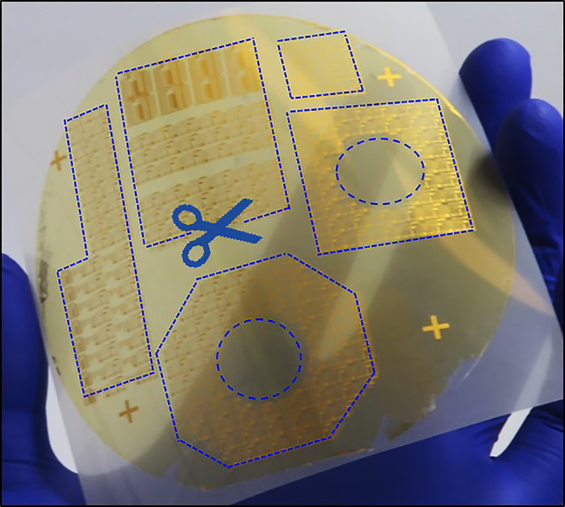
Researchers have designed peelable electronic films that can be cut and pasted onto any object to achieve desired functions. (Purdue University image/Chi Hwan Lee)
Filed Under: M2M (machine to machine)


