By John Bottrill, Senior Applications Engineer, Texas Instruments, Manchester, NH
Of the many possible ways to handle a feedback error signal in a control loop, the best decision is to use the integrated, error-amplifier output of the dedicated control IC, not an external error signal: The latter gives rise to several problems not immediately obvious.
Many design engineers use a feedback method that directly drives the output of the control IC’s error amplifier (COMP pin) rather than its input. This technique bypasses the control IC’s error amplifier and causes a few problems –neither obvious nor intuitive.
The wrong way
In this example, the feedback loop from the control system’s output or load to the input comparator contains an optical coupler. This is a generic opto-coupler and comes with a good deal of technical data for characterization.
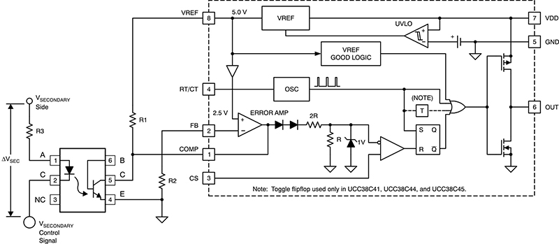
A feedback method that directly drives the COMP pin of the error amplifier (instead of the FB-pin input) can give less than optimal performance for a feedback control system and reveals some SNR (signal to noise ratio) problems with inferior unit-to-unit repeatability. (The UCC28C42 is the control IC chip used for this article. Its specifications can be found at http://www.ti.com/ucc28c42-ca.)
When directly controlling the COMP pin, the opto-coupler’s phototransistor collector connects between the controller IC’s COMP pin and ground. The resistor R1 also connects between the VREF and COMP pins. This provides an impedance for opto-coupler gain calculations. Another resistor connects the FB pin to ground, which forces the output of the amplifier (COMP pin) to go high.
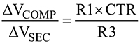
The opto-coupler’s voltage gain is then the resistance of the resistor from the VREF pin to the feedback pin (R1), times the CTR (current transfer ratio) of the opto-coupler, divided by the resistance of R3, which is in series with the photo diode:
Typically, the gain is a straightforward and easily determined value. It would be very simple to calculate if it were not for the opto-coupler and the ERROR AMP operational characteristics and limitations.
To understand this, look at the characteristics of the current mode controller (CMC). The COMP pin is the connecting point of a voltage-controlled current source and current sink. With the feedback pin (FB) connected to ground, the current source of the IC is fully on and the current sink is off. Without a load, the output of the ERROR AMP is at a high voltage and is trying to deliver current.
Look at UCC28C42 specifications: When the COMP pin is high at 5 V, it typically can source 1 mA – but this may be as little as 0.5 mA. The maximum current out of this pin is not specified, but the test program indicates a maximum of 5.0 milliamps. The specification sheet also states that the nominal “COMP-to-CS offset” is 1.15 V. This, too, will have a tolerance that will vary from chip-to-chip and over temperature. Tolerance from the test program indicates a range between 0.6 V and 1.7 V.
Assuming that R1 is 2.5 kΩ, the current through R1 will vary from zero up to 1.76 mA for a COMP voltage variation from 5 V to 0.6 V. Therefore, as determined from this information, the range of voltage and current for the opto-coupler phototransistor will vary from 5 V to about 0.6 V and the current will change from 0.5 mA (at COMP = 5 V and 0.5 mA out) to a maximum of 6.76 mA (at COMP = 0.6 V and 5.0 mA out). This is the current swing, taking into account all combinations of tolerances mentioned. To get zero duty cycle, the current through the transistor goes from 1.82 mA to 6.76 mA, depending on the “Comp-to-CS offset” tolerance and the variations in the current source of the COMP pin.
It is important to realize that of the 6.26 mA total differential (6.76 – 0.5) that the circuit must be able to handle, only 1.76 mA is related to the control function. The remaining 4.5 mA variations are due to the output current variations and tolerances in the current source of the ERROR AMP. This means that on the photo diode side of the opto-coupler, the voltage variations across the series resistor must have a minimum of this same ratio. By allowing for these tolerances, the signal-to-noise ratio (SNR) of this circuit is much lower than is desirable, even before considering the variations from the CTR.
This wide current swing from the variations in the current source of the UCC28C42 through the phototransistor results in a wide swing of current through the opto-coupler’s LED, which limits the dynamic voltage for the ?VSEC control signal to accomplish the control function.
Looking at the dynamics of the opto-coupler, the CTR can be between 100 and 200% for a 10 mA IF for the chosen typical opto-coupler. However, for an IF of 1 mA, the CTR drops to a minimum of 34. Another problem is the characteristics of the opto-coupler at low Vce voltages.
This opto-coupler diagram shows that for a Vce from about 1 V to 2.5 V, the CTR changes only slightly and is very nearly constant. However, as the voltage continues to drop, these variations increase. The collector current starts to roll off, which means the CTR starts to fall. Since the Vce in this feedback configuration needs to go as low as 0.6 V, this is a problem when the control loop circuit calls for zero duty cycle. Another problem is the variations of CTR with diode current.
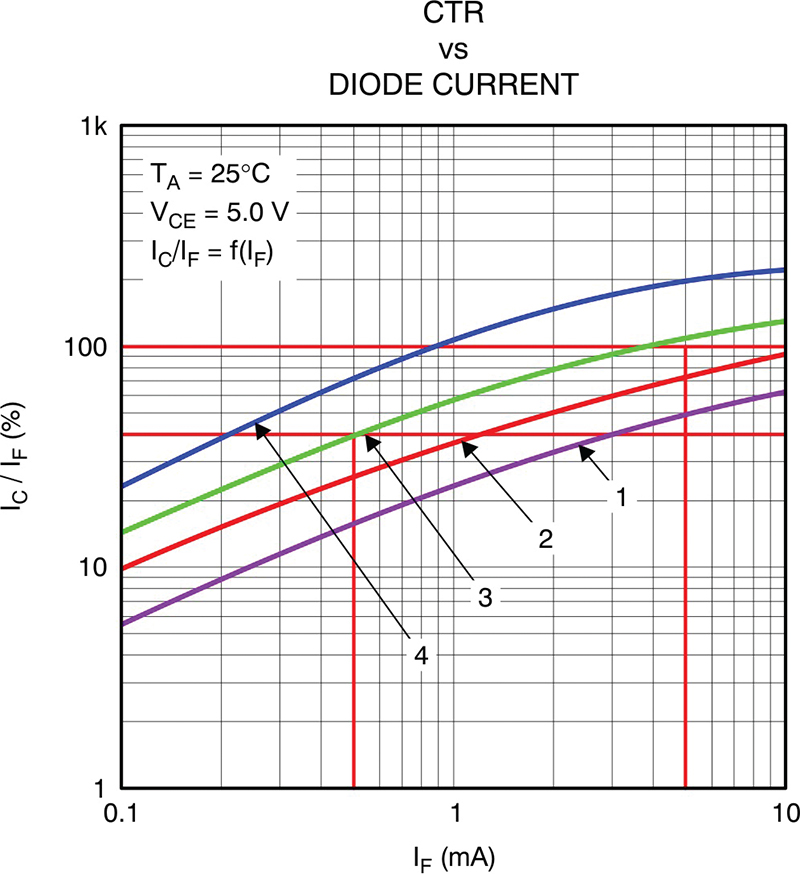
A major problem with the direct-drive circuit are the variations of CTR (current transfer ratio) with diode current.
For the opto-coupler, the CTR goes from about 40 to 100% for a variation in IF from 0.5 mA to 5.0 mA at a Vce of 5 V. All of these tolerances and variations add unwanted complexity to the design and require a wider dynamic range of the diode current to meet all possible combinations. A 40% CTR for a transistor current of 0.5 mA requires 1.25 mA of current through the photo diode. But for a transistor current of 6.76 mA and a CTR of 40%, the photo-diode current is approximately 17 mA. While at the other extreme of a 0.5 mA current through the transistor and a CTR of 100%, the required photo-diode current is only 0.5 mA.
However, the change in current through the transistor required for control is only 1.76 mA. At 100 % CTR, this is 1.76 mA through the photo diode, and 4.4 mA at a CTR of 40%. The minimum and maximum values are taken into account for all variables shown in Table 1:
TABLE 1
The minimum and maximum values for the various component values are conveniently arranged in this table to indicate the circuit performance.
Assuming that on the output side or load, the variable voltage available for control is 10 volts and a 400 Ohm resistor is used for this control, the voltage swing required is 6.76 V to cover all combinations of conditions. Depending on the CTR under worst-case conditions, 1.76 V (4.4 mA) of this 6.76 V is required for the control function, or about 26% of the total available range of the voltage swing. The other approximate 5 V of variation is needed to overcome the current variations of the COMP pin and the CTR variations. At the other extreme, where only 1.32 mA of current variations were needed, the dynamic control voltage requirement would be 0.53 V or less than 8%.
With a minimum voltage requirement of 0.6 V for the COMP to CS offset, the parameters of the opto-coupler and the COMP pin may prevent the pulse width of the converter from going to zero duty cycle over all line, load, and temperature conditions. This can be a serious problem.
The right way
The solution to most of the problems described above is to change the configuration and make use of the ERROR AMP within the IC to control the COMP voltage. The first thing to notice about the new configuration is that the current through R2 is always present and constant. The actions of the error amplifier cause the COMP pin and R1 to provide the necessary current to keep the FB pin at the same voltage as the internal 2.5 V reference. If R2 is set to 2.5 kΩ, then the current through R2 will be 1.0 mA continuous dc current.
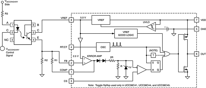
The right way (or at least a superior way) to use the error control amplifier in the IC is to drive the FB pin with an opto-coupler. It is much easier to use, more repeatable from unit-to-unit,
and has a better signal-to-noise ratio. It also has an added bonus in that it provides the control range necessary to shut down the converter when the output starts to climb out of the regulation window.
Next, the full range of voltage needed on the output of the COMP pin (0.6 V to 5 V) results in a current variation through the R1 (5 kΩ) of –0.5 mA to + 0.38 mA. When the COMP pin is high, 0.5 mA of current is supplied to R2 by R1, so the phototransistor (in the opto-coupler) only needs to source 0.5 mA. When the COMP pin is low, the phototransistor must source the 1 mA through R2 and the 0.38 mA through R1 or 1.38 mA total. This yields a total variation of 0.5 mA to 1.38 mA through the phototransistor. This 0.88 mA is the result of changes in the current through the phototransistor as a result of the control loop dynamics. The variations in the phototransistor have been reduced from 0.5 mA to 6.6 mA to a total variation from 0.5 mA to 1.38 mA.
This reduces the necessary transistor current swing to 14% of what it was in the previous case. It also fixes the voltage across the transistor to a constant 2.5 volts, which removes the extremely low operation that was present. At this current through the opto-coupler, the CTR is between 40 and 60%. At a CTR of 50%, the current through the photo diode is between 1.0 mA and 2.7 mA, or a change of 1.7 mA. Now that is 63% of the total current swing.
This lower current swing means a much better SNR because now 63% of the available voltage can be made up of control information as opposed to about 8% to 26% in the previous case. The entire variation in current is a result of signal changes, not offsets.
In summary, the design calculations required for the feedback loop as shown in the direct drive diagram are extremely complex when taking into account the variations in the parameters of the parts. It is much less complex when doing it the right way, using the loop in the FB-pin driven diagram. In addition, in this diagram, the SNR is much higher. Finally, the part count is the same, but the power consumption is much lower.
Discuss this on The Engineering Exchange:
Texas Instruments
www.ti.com
::Design World::
Filed Under: Packaging, ELECTRONICS • ELECTRICAL

Tell Us What You Think!