While working with delicate and expensive parts is an everyday task for advanced technology product manufacturers across myriad industries, perhaps more consideration can be given to the detail that goes into developing ways to protect, store, ship and handle such sensitive inventory as minuscule computer chips, tiny sensing devices, electronic subsystems, biotechnology components, optics and more.
The robustness and reliability of end products like medical devices, electronics, computers, automobiles, smartphones, wearables and even jewelry depends upon the robustness, reliability and overall quality of the parts inside them. As such, while they are seemingly simple and mundane, chip/device trays used to pack, store, ship and handle these parts are a critical part of the manufacturing ecosystem. Their function, design and material makeup can have a direct impact on product yield and overall cost of the goods they protect, including the level of success of the manufacturer. Choosing an off-the-shelf tray that might be sufficient versus designing a custom transport/storage tray that suits your specific needs could impact your bottom line (see Figure 1).
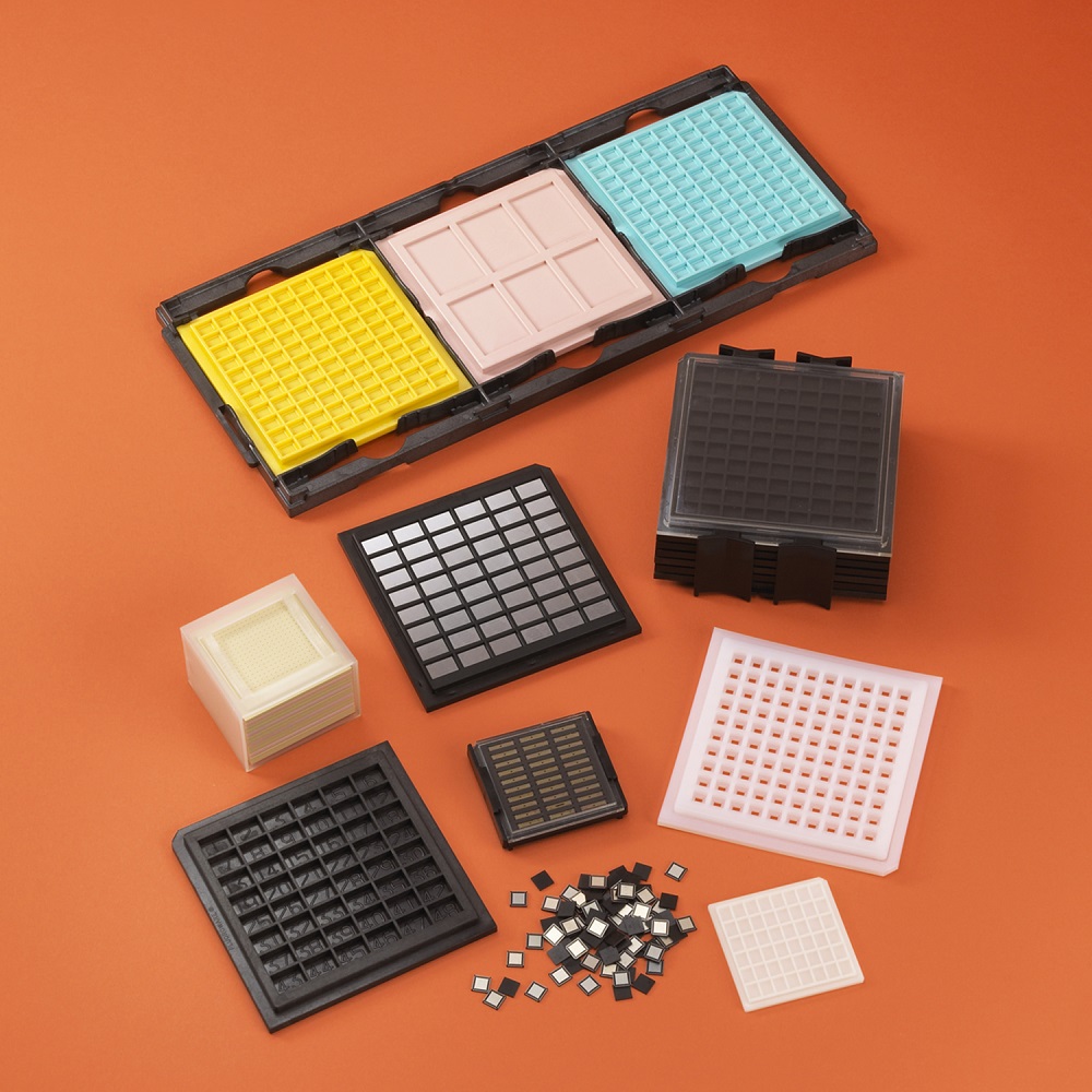
Figure 1: Samples of trays, sizes and devices.
For example, trays have been custom-designed for use in medical device manufacturing. There are many small components that go into robust and complex life-saving devices; therefore, these components must be in perfect condition for manufacturing. In a more exotic application, a tray for protecting, storing and shipping diamonds destined for a volume jewelry assembler may require custom pockets that protect these valuable gems. Or, more commonplace, miniature springs being shipped to a watch manufacturer might need to be held securely in place, even if they are dumped out on an assembly workstation upon arrival. What’s important is that all the parts arrive at their destination intact and without damage, and this can be accomplished by designing and using trays adequately suited to safely transport valuable items.
Although it may seem obvious that different industries would have product-handling specifications to ensure the best possible outcomes for their fragile devices, this isn’t always the case. Often, details about the device the tray is designated for cannot be fully disclosed; for example, the high-end smartphone for which the chip is the “secret sauce” or the sensor that contains manufacturing materials that sets it apart from its competitor.
There are, however, several critical parameters to consider when looking for the right chip/device/component tray design to suit a specific need.
Look for a Material Suited to Your Device’s Environment
Before a material can be recommended for a specific chip or device tray application, design engineers need to consider parameters such as the temperature of the storage and shipping environment, chemicals it may be exposed to, the surface resistivity of the chip/device, tray coatings used and special circumstances, such as whether it needs to be RoHS compliant.
For example, if the application requires static protection and dimensional stability, polycarbonate with carbon powder is recommended. If it also needs to have a colorable background, then an ABS alloy and intrinsically dissipative polymer are used. If dimensional stability is the sole requirement, then acrylonitrile butadiene with a color additive fits the bill. Alternatively, if static protection and less stringent dimensional stability is the goal, polypropylene with carbon and glass bead may be the right choice.
Look for Design Features That Offer the Best Protection
The questions most often asked about chip/device trays are, “Will my device fit in the tray pocket?” and, “Will it rotate or move around during shipping?” The good news is that, with custom designs, the right fit is designed directly into the tray, and the price/value equation for this type of solution today may pleasantly surprise you.
At a minimum, it’s important to provide accurate dimensions of a device to determine pocket size. A device needs to fit snugly into the pocket without incurring undue stress for it to be well-protected. Depending on the size and fragility of the chip/device, adding special features can increase protection. For example, corner relief features protect sharp, fragile corners of the component.
If the device needs to be cleaned while still in the tray, through-holes can be incorporated into the design to drain excess liquid. Through-holes can also be used if the tray will be under vacuum, to ensure the devices are held in place.
For small, delicate devices that can only be handled with tweezers, or for air circulation, tweezer slots are available. Further, if the device has a smooth surface, an electrical discharge machining (EDM) finish provides a rough texture created by microscopic peaks and valleys that reduce surface tension of the tray so chips don’t get stuck in the pocket. Additionally, an EDM finish results in a matte surface, which eliminates glare during the optical inspection.
Lastly, the thinness of the die or device can significantly impact a tray design. When devices are thinner than 2x the flatness of a tray, they might “jump” into other tray pockets, or scatter around the tray. This happens when the tray bows up to the flatness limit in one direction, and the cover or top tray bows in the opposite direction. This is called “part migration,” which can be prevented by including a hold-down feature in the cover design. Alternatively, if trays will be stacked, the bottom of the trays can be customized with hold-down features to secure the device in the tray pocket and prevent part migration (see Figure 2).
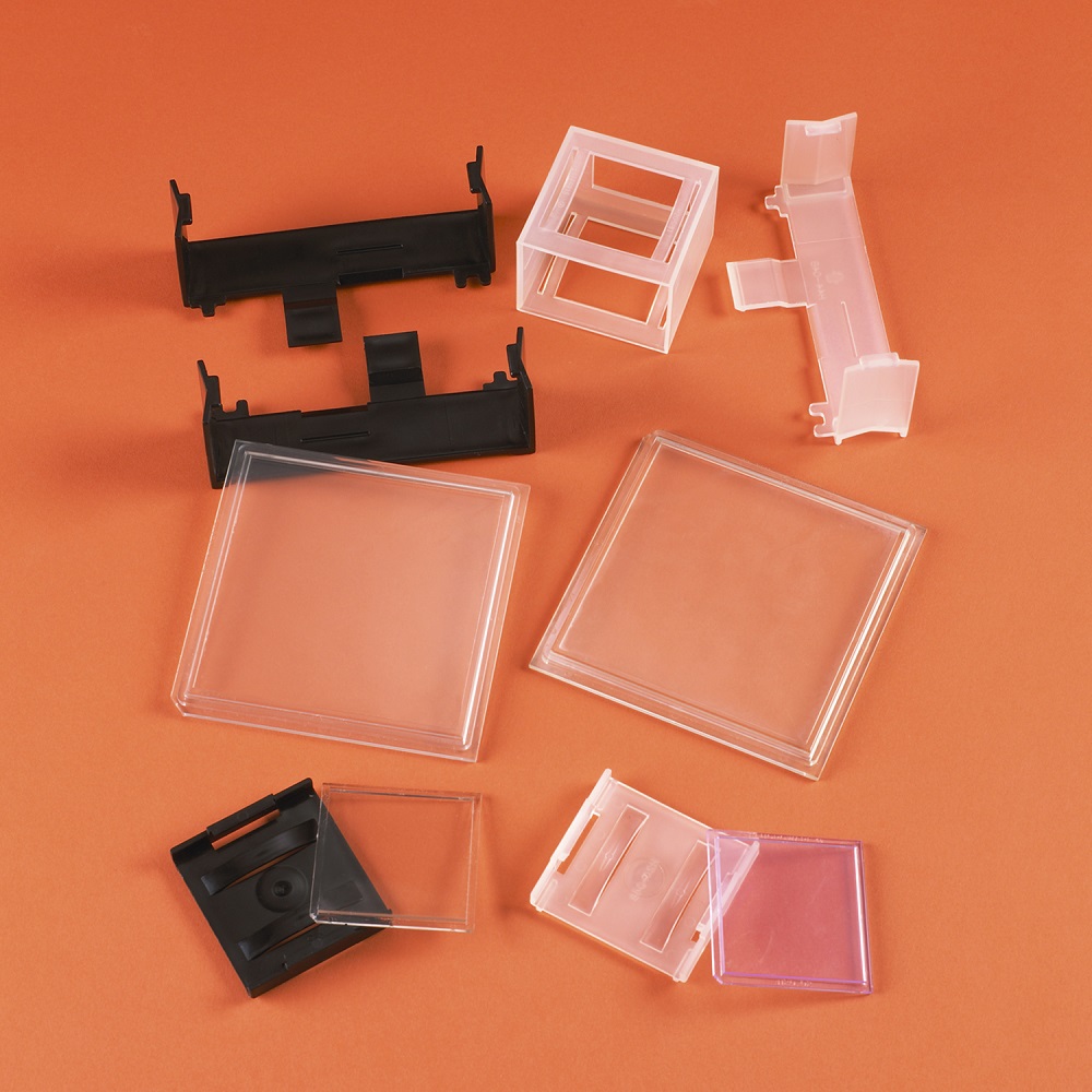
Figure 2: Accessories, like tray clips, holders and covers, can provide added protection during use and shipping.
Other Considerations That Impact Tray Design
From the perspective of the final assembly provider, these incoming devices may then need to be transferred to a tray that integrates with the final assembly tools. Understanding the full supply chain scenario can help design engineers customize the trays to accommodate these needs.
While custom trays may cost more than off-the-shelf versions, the potential impact on yield could drastically offset the added cost of a custom design. Trays of subpar quality, or those with molding defects, can damage delicate semiconductor chips or other fragile components placed in the trays.
One way to manage the cost of custom-designed trays is to avoid over-designing. Working in collaboration with a tray design engineer can help ensure the proper dimensions and features to suit your needs and your budget quickly and efficiently (see Figure 3).
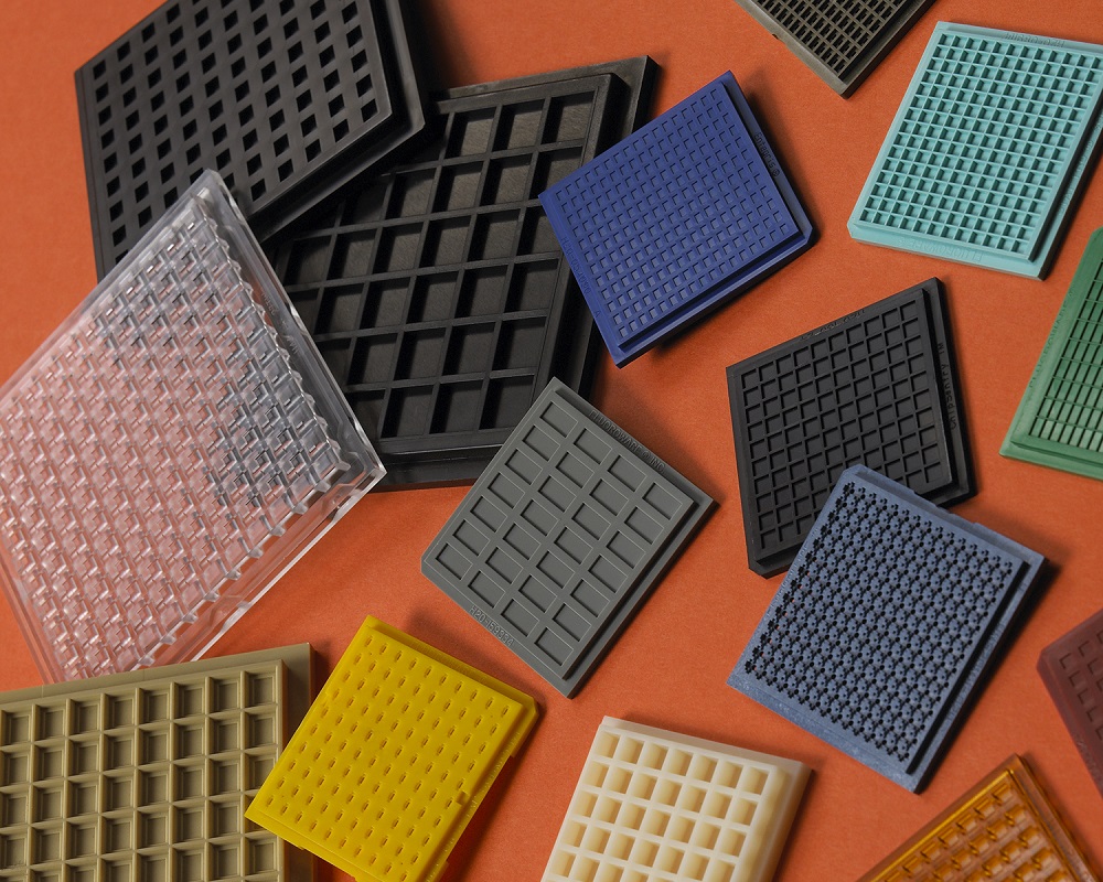
Figure 3: Trays can be customized to meet a variety of sizes and component needs.
Conclusion
A well-designed custom chip or device tray is a worthwhile investment to protect an even larger investment: costly components that took a good deal of time and energy to build. While the purpose of the tray may seem simple—to protect, store and ship, with the assurance that the devices arrive in one piece, ready for final assembly—customizing to ensure a high-yield outcome is not simple, but neither is it horribly complex with today’s capabilities.
The five most important things to look for in a carrier tray, therefore, are quality, consistency, dependability, predictability, fit and reliability. As a trusted provider of chip/device trays to a broad range of markets, Entegris has the in-house design experience to provide fully customized chip trays in as little as two weeks. In addition, Entegris offers an automated, online tray designer “wizard” that helps you design and see the tray that fits your device. For “off the shelf” options, Entegris carries one of the largest tray libraries in the world, at over 15,000 trays.
Filed Under: Materials • advanced