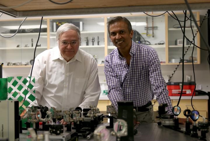
University of Utah physics and astronomy Distinguished Professor Valy Vardeny, left, and University of Utah electrical and computer engineering professor Ajay Nahata have discovered that a special kind of perovskite, a combination of an organic and inorganic compound that has the same structure as the original mineral, can be layered on a silicon wafer to create a vital component for the communications system of the future. Image credit: Dan Hixon/College of Engineering
A mineral discovered in Russia in the 1830s known as a perovskite holds a key to the next step in ultra-high-speed communications and computing.
Researchers from the University of Utah’s departments of electrical and computer engineering and physics and astronomy have discovered that a special kind of perovskite, a combination of an organic and inorganic compound that has the same structure as the original mineral, can be layered on a silicon wafer to create a vital component for the communications system of the future. That system would use the terahertz spectrum, the next generation of communications bandwidth that uses light instead of electricity to shuttle data, allowing cellphone and internet users to transfer information a thousand times faster than today.
The new research, led by University of Utah electrical and computer engineering professor Ajay Nahata and physics and astronomy Distinguished Professor Valy Vardeny, was published Monday, Nov. 6 in the latest edition of Nature Communications.
The terahertz range is a band between infrared light and radio waves and utilizes frequencies that cover the range from 100 gigahertz to 10,000 gigahertz (a typical cellphone operates at just 2.4 gigahertz). Scientists are studying how to use these light frequencies to transmit data because of its tremendous potential for boosting the speeds of devices such as internet modems or cell phones.
Nahata and Vardeny uncovered an important piece of that puzzle: By depositing a special form of multilayer perovskite onto a silicon wafer, they can modulate terahertz waves passing through it using a simple halogen lamp. Modulating the amplitude of terahertz radiation is important because it is how data in such a communications system would be transmitted.
Previous attempts to do this have usually required the use of an expensive, high-power laser. What makes this demonstration different is that it is not only the lamp power that allows for this modulation but also the specific color of the light. Consequently, they can put different perovskites on the same silicon substrate, where each region could be controlled by different colors from the lamp. This is not easily possible when using conventional semiconductors like silicon.
“Think of it as the difference between something that is binary versus something that has 10 steps,” Nahata explains about what this new structure can do. “Silicon responds only to the power in the optical beam but not to the color. It gives you more capabilities to actually do something, say for information processing or whatever the case may be.”
Not only does this open the door to turning terahertz technologies into a reality — resulting in next-generation communications systems and computing that is a thousand times faster — but the process of layering perovskites on silicon is simple and inexpensive by using a method called “spin casting,” in which the material is deposited on the silicon wafer by spinning the wafer and allowing centrifugal force to spread the perovskite evenly.
Vardeny says what’s unique about the type of perovskite they are using is that it is both an inorganic material like rock but also organic like a plastic, making it easy to deposit on silicon while also having the optical properties necessary to make this process possible.
“It’s a mismatch,” he said. “What we call a ‘hybrid.'”
Nahata says it’s probably at least another 10 years before terahertz technology for communications and computing is used in commercial products, but this new research is a significant milestone to getting there.
“This basic capability is an important step towards getting a full-fledged communications system,” Nahata says. “If you want to go from what you’re doing today using a modem and standard wireless communications, and then go to a thousand times faster, you’re going to have to change the technology dramatically.”
Filed Under: Materials • advanced