Two primary photovoltaic technologies are used to make solar energy modules: crystalline silicon and thin film. Crystalline silicon technology currently makes up about 80% of the market. This technology uses silicon wafers as its main raw material. The wafers are cut from cast ingots in very thin slices with a thickness in the range of 200 to 300 µm.

The finished solar panels are assembled into arrays, which are often servo-motor driven to maintain their position for maximum solar-energy collection.
In crystalline silicon manufacturing, the wafers are processed, interconnected, and laminated into a substrate, which is typically made of glass. Commercial grade solar modules using crystalline silicon technology can convert sunlight to useable electrical energy at a relatively high efficiency ranging from 14 to 19%. Although efficiency is good, this technology can be very expensive due to the high cost of the silicon wafers, which make up 40 to 50% of the price of the finished solar module.
Thin film technology accounts for the other 20% of the solar module market. This technology does not employ a silicon wafer as the active semiconductor layer in the solar cell. Instead, photovoltaic material is deposited in a very thin layer—typically with a thickness of 1 µm or less—to a glass substrate or a flexible thin metal or plastic substrate.
After deposition, the substrate is processed and separated into individual cells, which are connected in series. Thin film solar modules only achieve conversion efficiencies in the range of 8 to10%, but are much less expensive to manufacture because silicon wafers are not required as a raw material. The goal with both technology types is to drive efficiency up and costs down.
Solar Manufacturing Technology
A typical solar manufacturing line, either crystalline silicon or thin film, can be divided into two parts: front-end and back-end. The solar cells are fabricated in the front end of the process, and finished individual cells are assembled into larger solar modules in the back-end of the process. The crystalline silicon technology front-end process is very similar to that of a traditional semiconductor manufacturing line, so many equipment manufacturers that have traditionally serviced the semiconductor industry are now modifying their machine designs to accommodate the requirements of solar cell manufacturing.
The front-end process for producing thin film solar cells is generally proprietary and varies depending on the manufacturer, so that process is not presented here. Instead, crystalline silicon solar module manufacturing is examined.
Front End Processing
This diagram illustrates a typical crystalline silicon, front-end manufacturing line. (Courtesy of Spire Solar).
The manufacturing process starts with a texturing etch and ends with cell sorting. To simplify, there are three primary phases of the front-end process. In the first phase, each wafer is cleaned, saw damage is removed, and then the surface of each wafer is textured. Texturing reduces the amount of reflection and allows the wafer to absorb more sunlight, dramatically increasing cell efficiency. Following cleaning and texturing, an anti-reflective coating is deposited onto each wafer, which further increases the cell’s ability to absorb sunlight.
In the second phase of the front-end process, the wafers are screen printed with a pattern of bussing material used to collect the electrons that are generated from the photovoltaic material. The wafers are then cured in a furnace and cooled.
In the third and final phase, each finished cell is tested with simulated sunlight and sorted according to electrical performance. The finished cells then proceed to the back-end of the manufacturing process.
The back-end process begins with the preparation of the substrate. This substrate, typically made from glass, is used to encapsulate the cells that have just been tested following the front-end process. After the glass has been cleaned and layered with a sheet of ethylene vinyl acetate, cells are placed onto the glass. The cells are then interconnected by flat metal leads which are soldered in place by an automated tabber and stringer. The cells on the substrate then get laminated with a few layers of thermoplastic film. After lamination, the solar module cools and its edges are trimmed to the appropriate specification. A junction box is then added to the back of the module, and all of the necessary electrical connections between the box and the module are made via an automated process, usually involving some sort of custom robot. At this point, the solar module assembly is complete—and the module is tested with simulated sunlight and sorted based on electrical performance.
Drive costs down & efficiency up
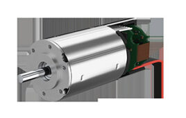
The efficiency of each manufactured solar module, which is typically 14 to 19% with crystalline silicon technology, can be increased by keeping tight control over each process. When the wafer is being processed in the front end manufacturing (cleaning, polishing, etching, texturing, and metalizing), it is crucial that the servo systems used to actuate the materials maintain a smooth and accurate motion profile. Servo amplifiers with the highest levels of bandwidth used with linear and rotary servomotors with high-resolution feedback devices are required to achieve these levels of accuracy. In order to maintain smooth motion, some servo amplifiers employ specific algorithms that stamp out machine vibration caused by natural resonance frequencies that occur during each process step. Use of these high-end servo systems allow solar module manufacturers to improve their overall product quality which in turn allows for higher energy conversion efficiencies.
Back End Processing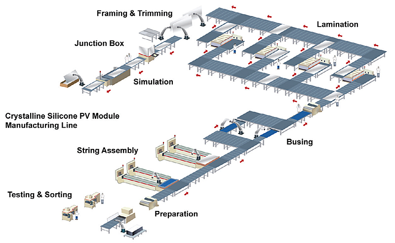
The back-end of a typical crystalline silicon solar cell manufacturing line is outlined in the diagram. The manufacturing process starts with preparation and ends with simulation, testing and sorting.
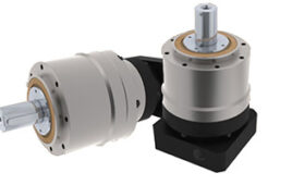
Driving down the manufacturing cost of each solar module is also a key factor in making solar power viable to the market. Increasing machine throughput is the primary way to reduce the cost of the end product. Solar module manufacturers work to improve cycle times and eliminate bottlenecks in their process in an attempt to produce more modules per hour. Employing technology like linear servo motors and high speed custom robots can assist in this effort. Towards that end, solar manufacturers often turn to vendors that can supply a full line of rotary, linear and direct drive servo motors and the engineering capability to design custom robotic solutions.
Discuss this on the Engineering Exchange:
Yaskawa America, Inc.
www.yaskawa.com
::Design World::
Filed Under: Green engineering • renewable energy • sustainability, Energy management + harvesting, Motion control • motor controls, ELECTRONICS • ELECTRICAL
Tell Us What You Think!