Today the Internet of Things (IoT) impacts almost all industries, with the potential to become a $1.7 trillion market by 2020. The IoT space is built on cloud computing and networks of data-gathering sensors with mobile, virtual, and instantaneous connectivity. Industry experts say this is going to make everything in our lives “smarter.”
IoT is already with us in a wide variety of industries, from factory automation to on-demand entertainment and wearable devices. Yet by most accounts, this huge interconnected system of intelligent devices has not reached its potential for changing the way we work.
The Internet of Things is undoubtedly the next growth driver for the semiconductor industry and embedded systems. The emergence of IoT is driving the need for many new enabling technologies including:
- Next-generation of ultra-low-power ICs
- New wireless communication protocols
- Advanced data processing technologies for analytics and cloud computing
As chips scale to smaller process nodes, one segment of the semiconductor industry that has been relatively hidden from view and is now becoming more visible is memory. The Internet of Things, with its exabytes of data flowing through the internet, is driving the need for high-performance memories that can also be low power and available in extremely small packages. Another constraint IoT has placed on semiconductors, and memories in particular, is the need for security and reliability. Vast amounts of private information will be stored in wearables, servers, and various other nodes of the Internet of Things.
For the last few decades, the memory space has been divided between two very distinct product families – fast and low-power – each with its own set of features, applications, and prices. Original equipment manufacturers can find memories that offer high performance so long as they are ready to sacrifice power consumption and even form factor in many cases. The converse is true for both volatile and non-volatile memories that have low power consumption.
The IoT trend, however, has changed memory requirements. Demand is growing for high-performance devices with low power consumption. These devices are required to perform complex operations while running on portable power. They must also minimize pin-count and form factor footprint. Microcontrollers have already adapted to this new set of requirements, by incorporating special low-power modes like Deep Power-Down and Deep-Sleep while providing iteratively better performance (i.e., clock frequency and feature set) with every generation. To keep up with these microcontrollers, memory will have to evolve in such a way that designers need not worry about a trade-off between performance and power.
In this article, we’ll focus on semiconductor memory trends for a space that has already begun to be influenced by IoT – retail shopping. This $2 trillion a year space has great potential for IoT to bring convenience to consumers. Retail is one of the most competitive industries in the world, with very tight margins and millions of retailers, all vying for a mature customer base. The large stores already use the Internet of Things to engage with their customer base and enable a shopping experience tailored to each individual shopper. Retailers are integrating devices with one another throughout the store, as well as with corporate headquarters and cloud resources. The ultimate goal is a connected store that leverages collected data to drive sales, build customer loyalty, manage inventory, and enhance operational efficiency.
Today, consumers use the internet extensively to influence their purchasing decisions, from researching products to shopping online and even writing product reviews. Retailers are behind consumers when it comes to using the internet in the shopping experience. To catch up, retailers are now making their stores more “intelligent” by linking physical and online aspects of retail so that every engagement is consistently rewarding.
Smart POS Terminals
One of the most visible examples of the impact the Internet of Things already has in retail is smart Point of Sale (POS) terminals. The POS terminal is in some ways the central node for the retailer to use IoT. Many leading “intelligent” stores use POS data to understand customer shopping trends, track inventory in real time, and in turn help online shoppers to accurately determine local product availability. This will also help retailers build custom offers for customers based on the frequency at which they shop for specific items.
To track the shopping statistics of individual shoppers, smart POS terminals are connected to scanners. This means smart POS terminals have to deal with data that’s many times larger than traditional POS terminals. Many of the newest models use the latest ARM processors running in GHz ranges. At the same time, most of these terminals are battery powered and portable, meaning these systems consume as little power as possible. Moreover, since the data that is transmitted is highly personal, there is a requirement for the highest level of data integrity, meaning stricter encryption standards are required than have traditionally been used. This is in addition to the standard fail-safe techniques (like lockout mode) that are used in all POS terminals.
POS terminals use multiple types of memories: Flash for non-volatile data storage of all sorts, DRAMs for caching, and SRAMs for microcontroller memory expansion or battery-backed configuration data logs. Sometimes even an external MMC is available. Figure 1 shows the block diagram of a typical POS terminal design. In order to meet the requirements of smart POS terminals, memories are expected to provide the highest level of reliability along with sufficient bandwidth. This also needs to be coupled with low power consumption and a small footprint in order to meet portability requirements.
Traditionally, memories have struggled to combine fast access times with low power consumption and small footprint. However, with the advent of new-generation low-pin-count interface like Octi-SPI and HyperBus™, there are now memories that can match or even exceed the bandwidth of fast access memories while rivaling the power consumption of low-power memories and using the lowest number of microcontroller pins. Another innovation that has carried over from microcontrollers to memories like SRAMs is the introduction of Deep-Sleep mode. For example, PowerSnooze™ SRAMs from Cypress are a type of Fast SRAM that has Deep-Sleep power efficiency comparable to Micropower SRAMs.
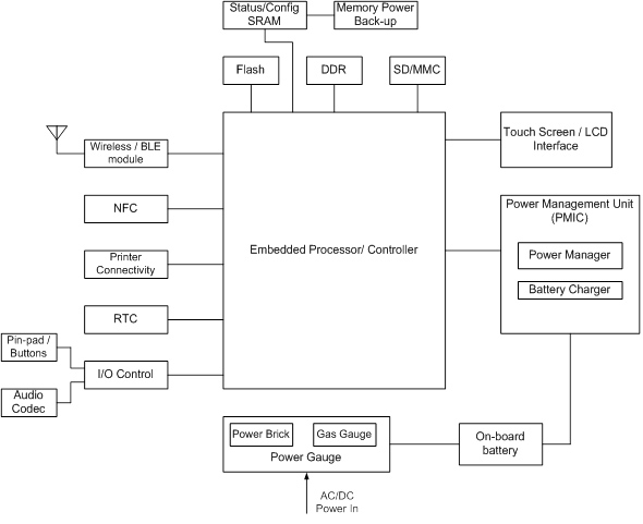
Figure 1. This is a block diagram of a modern POS terminal. The memories used are Flash, SRAM, DRAM, and SD/MMC slot.
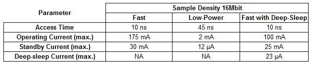
Let’s do a comparison of power and access time for the two common types of SRAMs – Fast and Micropower – and also a Fast SRAM with Deep-Sleep capabilities.
The combination of fast access and deep-sleep enables these memories to match the speed of Fast SRAM with excellent power efficiency on par with low-power SRAM. The advantage of this combination is more prominent in applications where the SRAM is on standby most of the time.
In a typical POS terminal that uses SRAMs for configuration data logging, the SRAMs are operational for only 20 percent of the time. If the SRAM is a Fast SRAM operating at 3.3V, it will consume 120 Watt-Hour (WH) during operation and 80 WH during standby. Total energy consumption comes in at 200 WH. With a Fast SRAM with Deep-Sleep, the energy consumption during operation remains 120 WH during operation, but the consumption during standby drops down to 0.06 WH. Thus, the total energy consumption is around 121 WH. In this particular case the Deep-Sleep option lowers energy consumption by 40 percent.
With an onboard 240mAH coin battery, a 16Mb Fast SRAM on standby will offer a battery life of over 12 hours. A low-power SRAM on standby, on the other hand, offers a battery life of over three years. However, it has the limitation of a slower access time. This is where a Fast SRAM with Deep-Sleep has significant advantage over low-power SRAMs, with over four times higher bandwidth (i.e., 10 ns access time vs. 45 ns access time) without a power penalty.
There is, however, one factor to consider when using deep-sleep mode, be it with an MCU or SRAM: the time to enter and exit deep-sleep mode. If the time interval between two active periods is too short in comparison to the time taken by the SRAM to enter or come out of deep-sleep mode, then the method will not be useful. This time interval is 300µs (max.), for example, with Cypress’s Fast SRAMs with Deep-Sleep. This could potentially be the biggest hurdle to the widespread adoption of SRAMs with deep-sleep mode.
Another interesting trend for memories is that as Flash memories are increasingly becoming faster, the need for a cache is changing. Many microcontroller processes that required a RAM can now be done on Flash using XIP (Execute In Place). This means that RAMs are increasingly required only as expansion memories or for battery backup. At the same time, the SRAMs which have been used for these two applications are growing in density options. That would mean that DRAMs, which are the traditional memories of choice, are becoming less relevant due to the combined powers of higher density, lower power, and more compact SRAMs for smaller memory needs like expansion memory, and faster, lower power Flashes for larger memory needs.
Other Components
There are many other components that comprise an intelligent shopping experience – various types of sensors, electronic shelf labels and beacons, and storage and data processing terminals. Discussing the applications and memory requirements of all these devices in a single article would be quite challenging. I plan to cover the memory requirements for these components in the near future. However, the underlying requirements remain largely unchanged – low-power, high-speed performance, small footprint, and high reliability.
You can learn more about SRAMs with deep-sleep mode by reading Power Saving SRAM. Further information on designing systems that are compatible with HyperFlash memories can be found in the Programmer’s Guide to HyperFlash Memories.
Reuben George works in Product Marketing for the Memory Products Division at Cypress Semiconductor. He holds a BE in Electrical & Electronics Engineering from the prestigious Birla Institute of Technology and Science (BITS), Pilani in Rajasthan, India.
Filed Under: Rapid prototyping