New software platforms can head off the subtle errors that sometimes creep into manual printed circuit board review processes.
David Wiens, Kerry Thalmann | Mentor Graphics, a Siemens Business
The growing complexity of printed circuit boards and multi-board products has rendered traditional design analysis and verification techniques obsolete. Manual reviews are no longer up to the task. Reliance on experts for all design analysis creates bottlenecks that delay project schedules.
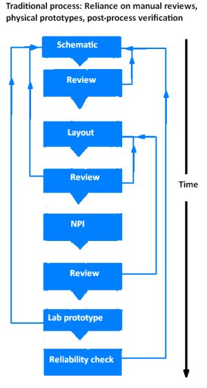
The traditional board design process usually starts with a schematic that gets turned into a PCB layout. The next step often takes place on a new product introduction (NPI) platform that handles PCB design-to-manufacturing handoffs. Next comes a prototype board that undergoes a reliability check before the design hits manufacturing. A point to note is that there are manual peer-reviews after each of these procedures.
It is easy for the complicated PCBs of today to contain a number of subtle errors that escape the notice even of experts in a traditional manual peer review process. It takes a modern, automated verification approach to catch schematic errors at the source. To reduce reliance on experts, the trend is to provide analysis tools that engineers who are non-specialists can use within their familiar design authoring environment. These modern approaches provide significant benefits for both design engineers and engineering project managers.
In the past, peer reviews done before PCB layout worked reasonably well for simple designs on a single PCB. This manual process became unwieldy for bigger designs. Schematic errors that got past the manual review went into PCB layout. They often remained undetected until the prototyping phase. These errors typically caused failures that require lab debugging time to identify the root cause. Errors that should have been caught prior to layout, where they are easily corrected, ended up causing costly design re-spins.
To eliminate such inefficiencies, design automation providers now advocate what’s called a shift-left approach. The idea is to integrate verification earlier in the design process. The benefit is an increased likelihood of catching errors and potential issues at the source, before they can propagate forward into subsequent phases of the project.
In the shift-left approach, automated schematic integrity analysis replaces manual reviews. It enables full inspection of all nets in the design, for both single and multi-board systems. It makes this inspection using pre-defined checks for common schematic errors and an intelligent component model library. The analysis takes place in parallel with schematic entry and eliminates most common schematic errors before layout starts.
Typical problems that verification can expose include missing power and ground connections, incorrect diode orientation, missing or redundant pull-up and pull-down resistors, capacitor voltage derating, nets missing a driver or receiver, driver/receiver technology matching, board-to-board connectivity, bus flip errors (MSB to LSB), etc. Replacing the manual review process with an automated methodology results in greater coverage and gives design engineers a much higher probability of entering layout with a schematic that will provide first-pass success.
Automated verification can also force good PCB design practices. Routing constraints for signal and power integrity, as well as design-for-test constraints, are factors that should be specified during schematic capture, not shoe-horned in at the layout phase. Signal and power integrity, EMI compliance, thermal analysis and vibration analysis should all be validated during the layout process.
Multi-dimensional verification schemes include a broad range of analysis and verification tools deployed during the schematic and layout phases of the project. These tools are simple enough to be used by non-specialist PCB design engineers and layout designers. These individuals can work within the authoring environments they’re familiar with to identify potential problems as early as possible in the design flow.
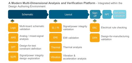
A modern multi-dimensional analysis and verification platform undertakes a number of analysis steps in the schematic and layout phases of board development as a means of reducing the need for input from human engineering specialists and to reduce the need for design re-spins caused by over-looked problems in the initial board design.
During schematic capture, automated schematic integrity analysis takes place to eliminate common errors often overlooked in manual reviews. Signal integrity and power integrity analysis takes place to determine a set of placement and routing constraints. The constraints get passed forward to layout. Also advisable during schematic entry is a testability analysis. Here, the software identifies test-point requirements and passes them to layout as additional constraints.
Several analyses take place as component placement progresses during layout. These analyses include EMI validation, thermal analysis, vibration/acceleration, and manufacturability assessments. In traditional design flows, these issues might only emerge after physical testing in EMI, thermal or HALT test chambers. Issues not caught during layout that impact the mechanical integrity of the design are usually the most expensive and time-consuming to fix. Such issues often require board re-spins and tooling changes to correct. Simulations during layout greatly boost the likelihood of avoiding such difficulties and getting first-pass success.
All in all, a shift-left verification process significantly improves the design before it reaches the PCB specialist. It greatly reduces the need for exhaustive full-board screening and lets these specialists focus on just the critical second-order issues that remain.
Engineering project managers
The traditional design flow is frustratingly unpredictable thanks to the many sources of potential problems. As a result, experienced managers typically bake at least one design spin into the project schedule, but even that is rarely enough to cover all contingencies.
Studies show (Lifecycle Insights – September 2018) the typical project using the traditional process flow goes through 2.9 re-spins, with an average schedule hit of 8.5 days and a cost of $44,000 per re-spin. For high-performance designs, the costs are often much higher. Thus the traditional approach wastes time, talent, materials, and puts projects at risk for cancelation.
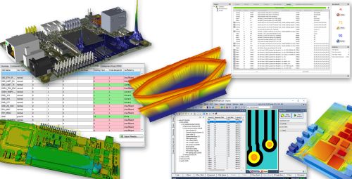
Screen shots from the Xpedition platform depict integrated testability analysis (left), automated schematic verification (top), and concurrent design-for-manufacturing analysis that takes place during board layout (bottom). Previously, these procedures would likely have taken place later in the board design cycle, perhaps making necessary changes more costly.
Clearly, traditional methods can result in the discovery of problems late in the project that can put the schedule at risk. In such emergencies, engineering “tiger teams” are often assembled by pulling engineers off other projects, delaying those project schedules. Technicians often must put in overtime to rework and test boards. Any additional board spins or mechanical design changes required this late in the game bring expensive rush charges. Last minute surprises can bring schedule delays and expanded project budgets. The left-shift approach invokes verification and analysis at an earlier point in the schedule to eliminate these last-minute surprises.
A reliance on engineering specialists can also bring schedule delays. These individuals are always in high demand and often support multiple projects concurrently. But bottlenecks caused by reliance on specialists can all but cease when design authors get powerful, easy to use analysis tools. Designers themselves can significantly improve the quality of the design before it reaches the specialist, reducing the need for exhaustive full-board screening by experts.
A shift-left methodology demands a fully-inclusive system design platform for upfront design analysis and verification. Mentor, a Siemens business, is the first electronic design software company with a broad portfolio of proven technologies to enable shift-left design verification.
The fully-integrated Xpedition verification platform for single and multi-board PCB system design includes automated schematic integrity analysis with built-in automated design checks and an extensive library of intelligent models. Testability analysis, automated component modeling for vibration analysis, dc voltage drop analysis for rigid-flex and multi-board designs, as well as concurrent DFM analysis during layout, are additional technologies integrated within the authoring environment for easier, faster validation. The benefits of this new multi-dimensional verification platform are the reduction of costly design re-spins, improved time-to-market for new products, and the development of higher quality products with fewer defects.
You may also like:
Filed Under: MOTION CONTROL, ELECTRONICS • ELECTRICAL, Analog IC Tips

