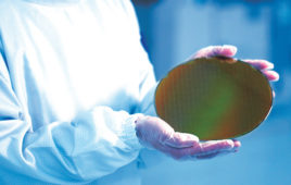
Patterning materials and processes are increasingly vital to high performance logic and memory devices. Traditional photoresists have been replaced by systems that allow for a five times thinner patterning stack, with thickness uniformity and defect levels compatible with 32 nm manufacturing.
The Applied Endura Metal Hardmask system with Versa TTN PVD technology delivers TiN1 hardmask film for patterning copper/low k interconnects and high aspect ratio contact structures. This metal hardmask film enables CD2 and profile control and preserves the k-value of ultralow k dielectric materials for increased chip speed and yield. The system is for high volume manufacturing at the 45 nm and 32 nm nodes and has a throughput to 85 wafers per hour.
“For dielectric films with k-values less than 2.5, the metal hardmask patterning sequence lets customers realize lower effective k-values by minimizing physical damage to the dielectric and reducing the thickness requirement for the underlying barrier film, ” said Dr. Farhad Moghadam, senior vice president and general manager of Applied Materials’ Thin Films Group.
Leading manufacturers have already qualified the hardmask system for 65 nm manufacturing. Its uniformity and productivity advancements ensure it will extend to the 32 nm node and to double-patterning sequences. Applied’s portfolio of advanced patterning films also includes the APF/DARC film stack, which combines the APF amorphous carbon hardmask film with a dielectric anti-reflective layer for advanced STI, gate and contact applications.
Applied Materials, Inc.
www.appliedmaterials.com
:: Design World ::
Filed Under: Semiconductor manufacture


Tell Us What You Think!