Design World

  • Home
  • Technologies
    • ELECTRONICS • ELECTRICAL
    • Fastening • joining
    • FLUID POWER
    • LINEAR MOTION
    • MOTION CONTROL
    • SENSORS
    • TEST & MEASUREMENT
    • Factory automation
    • Warehouse automation
    • DIGITAL TRANSFORMATION
  • Learn
    • Tech Toolboxes
    • Learning center
    • eBooks • Tech Tips
    • Podcasts
    • Videos
    • Webinars • general engineering
    • Webinars • Automated warehousing
    • Voices
  • LEAP Awards
  • 2025 Leadership
    • 2024 Winners
    • 2023 Winners
    • 2022 Winners
    • 2021 Winners
  • Design Guides
  • Resources
    • Subscribe
    • 3D Cad Models
      • PARTsolutions
      • TraceParts
    • Digital Issues
      • Design World
      • EE World
    • Engineering diversity
    • Trends
  • Supplier Listings
  • Advertise
  • Subscribe

NRL Clarifies Valley Polarization for Electronic and Optoelectronic Technologies

By Naval Research Laboratory | October 20, 2017

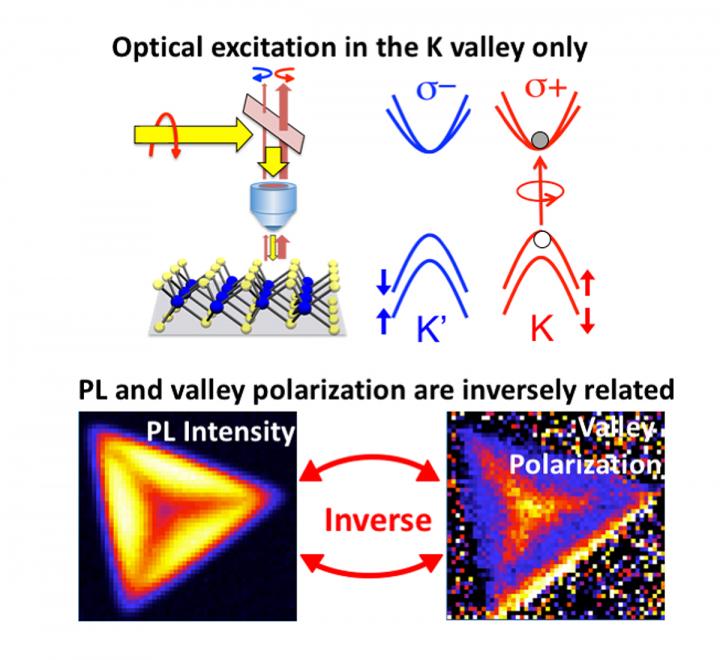
Upper Panel: schematic of optical excitation in the K valley of WS2 monolayers. Lower Panel: Photoluminescence (PL) intensity map of a triangular monolayer island of WS2 and the associated valley polarization map demonstrate the clear inverse relationship. Each map covers a 46 x 43 micron area. The regions exhibiting smallest PL intensity and lowest quality are found at the center of the flake and radiate outward toward the three corners. These regions correspond to the highest valley polarization. Image credit: US Naval Research Laboratory

An interdisciplinary team of scientists at the U.S. Naval Research Laboratory (NRL) has uncovered a direct link between sample quality and the degree of valley polarization in monolayer transition metal dichalcogenides (TMDs). In contrast with graphene, many monolayer TMDs are semiconductors and show promise for future applications in electronic and optoelectronic technologies.

In this sense, a ‘valley’ refers to the region in an electronic band structure where both electrons and holes are localized, and ‘valley polarization’ refers to the ratio of valley populations — an important metric applied in valleytronics research.

“A high degree of valley polarization has been theoretically predicted in TMDs yet experimental values are often low and vary widely,” said Kathleen McCreary, Ph.D., lead author of the study. “It is extremely important to determine the origin of these variations in order to further our basic understanding of TMDs as well as advance the field of valleytronics.”

Many of today’s technologies (i.e. solid state lighting, transistors in computer chips, and batteries in cell phones) rely simply on the charge of the electron and how it moves through the material. However, in certain materials such as the monolayer TMDs, electrons can be selectively placed into a chosen electronic valley using optical excitation.

“The development of TMD materials and hybrid 2D/3D heterostructures promises enhanced functionality relevant to future Department of Defense missions,” said Berend Jonker, Ph.D., principal investigator of the program. “These include ultra-low power electronics, non-volatile optical memory, and quantum computation applications in information processing and sensing.”

The growing fields of spintronics and valleytronics aim to use the spin or valley population, rather than only charge, to store information and perform logic operations. Progress in these developing fields has attracted the attention of industry leaders, and has already resulted in products such as magnetic random access memory that improve upon the existing charge-based technologies.

The team focused on TMD monolayers such as WS2 and WSe2, which have high optical responsivity, and found that samples exhibiting low photoluminescence (PL) intensity exhibited a high degree of valley polarization. These findings suggest a means to engineer valley polarization via controlled introduction of defects and nonradiative recombination sites

“Truly understanding the reason for sample-to-sample variation is the first step towards valleytronic control,” McCreary said. “In the near future, we may be able to accurately increase polarization by adding defect sites or reduce polarization by passivation of defects.”

Results of this research are reported in the August 2017 edition of the American Chemical Society’s Nano, The research team is comprised of Dr. Kathleen McCreary, Dr. Aubrey Hanbicki, and Dr. Berend Jonker from the NRL Materials Science and Technology Division; Dr. Marc Currie from the NRL Optical Sciences Division; and Dr. Hsun-Jen Chuang who holds an American Society for Engineering Education (ASEE) fellowship at NRL.

You Might Also Like


Filed Under: Materials • advanced


LEARNING CENTER

Design World Learning Center
“dw
EXPAND YOUR KNOWLEDGE AND STAY CONNECTED
Get the latest info on technologies, tools and strategies for Design Engineering Professionals.
Motor University

Design World Digital Edition

cover

Browse the most current issue of Design World and back issues in an easy to use high quality format. Clip, share and download with the leading design engineering magazine today.

EDABoard the Forum for Electronics

Top global problem solving EE forum covering Microcontrollers, DSP, Networking, Analog and Digital Design, RF, Power Electronics, PCB Routing and much more

EDABoard: Forum for electronics

Sponsored Content

  • Sustainability, Innovation and Safety, Central to Our Approach
  • Why off-highway is the sweet spot for AC electrification technology
  • Looking to 2025: Past Success Guides Future Achievements
  • North American Companies Seek Stronger Ties with Italian OEMs
  • Adapt and Evolve
  • Sustainable Practices for a Sustainable World
View More >>
Engineering Exchange

The Engineering Exchange is a global educational networking community for engineers.

Connect, share, and learn today »

Design World
  • About us
  • Contact
  • Manage your Design World Subscription
  • Subscribe
  • Design World Digital Network
  • Control Engineering
  • Consulting-Specifying Engineer
  • Plant Engineering
  • Engineering White Papers
  • Leap Awards

Copyright © 2025 WTWH Media LLC. All Rights Reserved. The material on this site may not be reproduced, distributed, transmitted, cached or otherwise used, except with the prior written permission of WTWH Media
Privacy Policy | Advertising | About Us

Search Design World

  • Home
  • Technologies
    • ELECTRONICS • ELECTRICAL
    • Fastening • joining
    • FLUID POWER
    • LINEAR MOTION
    • MOTION CONTROL
    • SENSORS
    • TEST & MEASUREMENT
    • Factory automation
    • Warehouse automation
    • DIGITAL TRANSFORMATION
  • Learn
    • Tech Toolboxes
    • Learning center
    • eBooks • Tech Tips
    • Podcasts
    • Videos
    • Webinars • general engineering
    • Webinars • Automated warehousing
    • Voices
  • LEAP Awards
  • 2025 Leadership
    • 2024 Winners
    • 2023 Winners
    • 2022 Winners
    • 2021 Winners
  • Design Guides
  • Resources
    • Subscribe
    • 3D Cad Models
      • PARTsolutions
      • TraceParts
    • Digital Issues
      • Design World
      • EE World
    • Engineering diversity
    • Trends
  • Supplier Listings
  • Advertise
  • Subscribe
We use cookies to personalize content and ads, to provide social media features, and to analyze our traffic. We share information about your use of our site with our social media, advertising, and analytics partners who may combine it with other information you’ve provided to them or that they’ve collected from your use of their services. You consent to our cookies if you continue to use this website.OkNoRead more