Design World

  • Home
  • Technologies
    • 3D CAD
    • Electronics • electrical
    • Fastening & Joining
    • Factory automation
    • Linear Motion
    • Motion Control
    • Test & Measurement
    • Sensors
    • Fluid power
  • Learn
    • Ebooks / Tech Tips
    • Engineering Week
    • Future of Design Engineering
    • MC² Motion Control Classrooms
    • Podcasts
    • Videos
    • Webinars
  • LEAP AWARDS
  • Leadership
    • 2022 Voting
    • 2021 Winners
  • Design Guide Library
  • Resources
    • Subscribe!
    • 3D Cad Models
      • PARTsolutions
      • TraceParts
    • Digital Issues
      • Design World
      • EE World
    • Women in Engineering
  • Supplier Listings

On-Chip Pumps Achieve High-Speed Sorting Of Large Cells

By Nagoya University | July 28, 2017

Share

A research group in Nagoya University developed a high-speed cell sorting method of large cells with high-viability using dual on-chip pumps.

The sorting of individual cells is necessary for many biological applications, including the isolation of specific cell types from cell suspensions. A fluorescence-activated cell sorting (FACS) has been used for high-throughput cell sorting. In this method, lasers are used to excite auto-fluorescence or tagged-fluorescence of cell included in droplets, and then droplets are diverted into different containers depending on their characteristics. However, this technique is concerned about sample infections due to aerosols generation. Additionally, a FACS of larger cells requires the samples to be processed under low pressure through wider nozzles to prevent damage. Thus, sorting is limited to low-level throughput.

Research at Nagoya University on cell sorting used a microfluidic chip to prevent sample infection. This chip has microchannels into which cell suspensions are introduced for sorting. The research group integrated two externally-driven on-chip pumps into the microfluidic chip for high-speed flow control. Using a high-speed actuator as the driving source of pump, they succeeded in producing a flow with 16 microseconds for cell sorting.

Microfluidic chip contains a cross-shaped sorting area and three-branched microfluidic channel. “Target/non-target cells are three-dimensionally aligned in the main channel,” corresponding author Shinya Sakuma says. “When target cells are detected, the on-chip pumps work rapidly to sort cells into one of two interest channels. Meanwhile, non-target cells are flushed into the waste channel without pump actuation.”

The technique allows us to sort not only large but also small cells with high speed, high purity, and high viability. “We tested the method on microalgae as an example of large cells, around 100 micrometers in size, and achieved 95.8 percent purity, 90.8 percent viability, and a 92.8 percent success rate,” corresponding co-author Yusuke Kasai says. “As a model small cell type, we used a cancer cell whose size is around 24 micrometers, and achieved 98.9 percent purity, 90.7 percent viability, and a 97.8 percent success rate.”

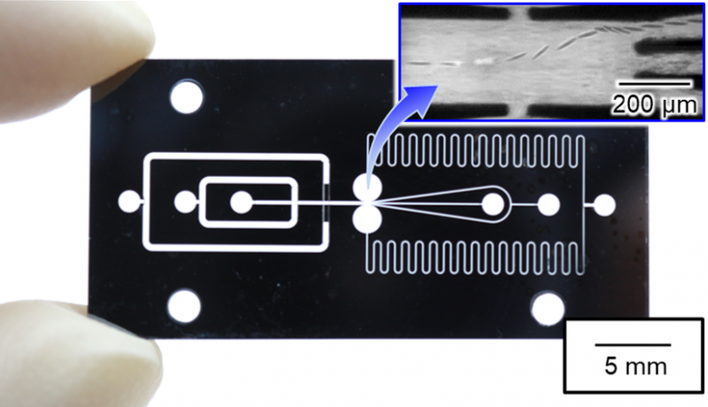
The photograph shows the developed microfluidic chip which enables us to sort cells at high speed of 16 microseconds. The enlarged view shows a demonstration of on-chip cell sorting of a Euglena gracilis cell (time interval of each frame: 40 μs). © Shinya Sakuma, Yusuke Kasai, Takeshi Hayakawa, and Fumihito Arai (Image Credit: Nagoya University)


Filed Under: M2M (machine to machine)


Related Articles Read More >

Part 6: IDE and other software for connectivity and IoT design work
Part 4: Edge computing and gateways proliferate for industrial machinery
Part 3: Trends in Ethernet, PoE, IO-Link, HIPERFACE, and single-cable solutions
Machine Learning for Sensors

DESIGN GUIDE LIBRARY

“motion

Enews Sign Up

Motion Control Classroom

Design World Digital Edition

cover

Browse the most current issue of Design World and back issues in an easy to use high quality format. Clip, share and download with the leading design engineering magazine today.

EDABoard the Forum for Electronics

Top global problem solving EE forum covering Microcontrollers, DSP, Networking, Analog and Digital Design, RF, Power Electronics, PCB Routing and much more

EDABoard: Forum for electronics

Sponsored Content

  • Industrial disc pack couplings
  • Pushing performance: Adding functionality to terminal blocks
  • Get to Know Würth Industrial Division
  • Renishaw next-generation FORTiS™ enclosed linear encoders offer enhanced metrology and reliability for machine tools
  • WAGO’s smartDESIGNER Online Provides Seamless Progression for Projects
  • Epoxy Certified for UL 1203 Standard

Design World Podcasts

July 26, 2022
Tech Tuesdays: Sorbothane marks 40 years of shock and vibration innovation
See More >
Engineering Exchange

The Engineering Exchange is a global educational networking community for engineers.

Connect, share, and learn today »

Design World
  • Advertising
  • About us
  • Contact
  • Manage your Design World Subscription
  • Subscribe
  • Design World Digital Network
  • Engineering White Papers
  • LEAP AWARDS

Copyright © 2022 WTWH Media LLC. All Rights Reserved. The material on this site may not be reproduced, distributed, transmitted, cached or otherwise used, except with the prior written permission of WTWH Media
Privacy Policy | Advertising | About Us

Search Design World

  • Home
  • Technologies
    • 3D CAD
    • Electronics • electrical
    • Fastening & Joining
    • Factory automation
    • Linear Motion
    • Motion Control
    • Test & Measurement
    • Sensors
    • Fluid power
  • Learn
    • Ebooks / Tech Tips
    • Engineering Week
    • Future of Design Engineering
    • MC² Motion Control Classrooms
    • Podcasts
    • Videos
    • Webinars
  • LEAP AWARDS
  • Leadership
    • 2022 Voting
    • 2021 Winners
  • Design Guide Library
  • Resources
    • Subscribe!
    • 3D Cad Models
      • PARTsolutions
      • TraceParts
    • Digital Issues
      • Design World
      • EE World
    • Women in Engineering
  • Supplier Listings