By Nolan Johnson, CAD/EDA Manager, Sunstone Circuits
How efficient is your PCB manufacturing designer?
When a design team puts their first prototype onto the workbench for testing and verification, the team must simultaneously debug the following:
• The concepts in the schematic design
• The layout’s implementation of the concepts
• The behavior of any firmware/software onboard
• The ability of the chosen parts to interact as expected from the component datasheet documentation, functional specifications, and schematic-driven simulation data
• The fabricator’s ability to manufacture what the layout instructed them to build
That’s a lot to debug, all at the same time. The more a manufacturing provider can shorten this list for the design team, the better. The more the board fabricators can remove debugging discussions that start with “I found a short in the board you built me,” the more the board manufacturer can help the design team target functional behaviors, instead of build errors; resulting in a shortening of the product design cycle.
Design flows are a key contributor to the efficiency of the electronic product development cycle. But, one needs to look a little deeper to realize that the prototype fabrication portion of the process is critical in catching design errors early and effectively. It is the prototype hardware, after all, which verifies the original design intent embodied by the CAD file contents.
Optimization for production
Close attention to design issues increases the overall manufacturing yield of the end product. Designing for durability also helps promote yield. It is a good idea to implement the same design ideas during prototyping, but with different target criteria. Here are key factors to strive for:
• Production designs optimized for volume production
• Prototypes optimized for quick turns
• Production optimized for component costs
•Prototypes optimized for functional verification
• Production designs that reduce manufacturing costs
• Prototypes that reduce design errors
Manufacturing quality has a decided impact on prototyping and small-run board Return on Investment (ROI.) A Printed Circuit Board (PCB) manufacturing process can greatly affect individual design teams.
Manufacturing quality can be defined as:
• Schedule adherence (on-time delivery)
• Design adherence
• Accessibility
• Yield
These four factors affect the manufacturing quality of a prototype PCB project.
1. Schedule adherence
Delivery schedule adherence (DSA) is used to calculate the timeliness of deliveries from suppliers. On-time delivery results in less expense to the customer’s design team. Occasionally, PCB’s are manufactured to a schedule; yet, the carrier causes delays outside the scope of both the manufacturer and the customer. In an effort to avoid delivery conflicts, a shortened prototype design phase overall, and a more cost-effective development project should be considered in the product development cycle.
2. Design adherence
Design adherence is the ability of the manufacturer to build exactly the board that the designer created. There are factors that can prevent design adherence such as, tolerances, machine processes, materials, and so on. Strict adherence is not always possible in the real world.
It is important to identify design adherence issues. Violations in design adherence can be debugged back to unintentional problems, opens or shorts in the PCB itself, or caused by manufacturing issues. These problems could be caused by components that do not perform exactly as specified in the data sheet; such as a flaw in the circuit design itself.

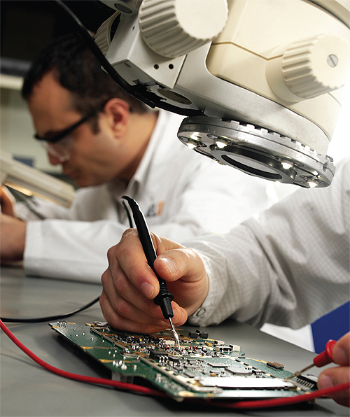
Design Adherence is the ability of the manufacturer to build exactly the board that the designer created. photo:sunstone circuits
One example is the Motorola Razr cell phone in 2006. Two days before the device was released for sale, some savvy cell phone sales reps noticed that the stock of factory-refurbished devices was abnormally high. Since the Razr hadn’t even gone on sale yet, these factory-refurbished devices couldn’t have come from customer returns. Instead, these were likely reworked devices that failed final QC at the factory. Concluding that such a high failure rate at the factory would translate to a high-failure phone in the field, these astute sales reps advised customers to hold off on purchasing that particular phone. The reps were worried about a potential onslaught of customer returns and the expense that goes along with handling each return/exchange. In early 2006, faced with a high rate of customer returns, some cell carriers’ halted sales of the Razr altogether. The problem ultimately was traced to a faulty component, and resolved at the production facility.
The type of issue experienced by the Razr in 2006, cannot always be caught in prototype, but some issues can be caught. In the prototype phase, design adherence helps the design team concentrate on the behavior of the design during debugging, not on whether the PCB manufacturer built what the design team specified.
Another example is based on a standard return merchandise authorization (RMA) rate of about 2% for PCB manufacture and costs of $1,000/day in design team costs for each day of delay. A firm generating 1,000 orders per day of prototype boards, should expect to generate about 20 customer rebuilds daily. If the RMA rebuild requires 3 days to get to the customer, then design teams lose $60,000, cumulatively, per day to manufacturing RMA. An RMA rate of less than 1% would translate to an RMA-related loss one-third of the baseline established. Such an RMA rate annualizes to almost $10 million dollars of saved customer R&D budget.
Just as the Razr example demonstrates that one can rate a product’s quality in part by examining the RMA rates, one can also get a feel for a prototype PCB manufacturing partner from their RMA rates. To do so, a manufacturer’s ability to transform CAD files into a prototype (Quick-turn manufacturing process) with a low level of RMA work shows that a manufacturer brings extra value by: 1) clearly and proactively publishing its Quick-turn manufacturing criteria; 2) providing tools and utilities that design teams can use to incorporate the Quick-turn criteria from design start; 3) ensuring said manufacturer complies with all customer-supplied production manufacturing instructions; and, 4) offering design reviews by request.
3. Accessibility
The role of a prototype-manufacturing partner is a collaborative one and accessibility is critical in the product development cycle. It is important to your overall productivity that your schedule and terms can be met. With current global business practices, the design team may be on a very different time schedule from the manufacturing facility. Although, it might be tolerable to work with 16 hour time differences to the production facility, the prototype manufacturing provider needs to be much more accessible than the production facility. If your PCB partner isn’t available for technical assistance during unconventional times, the design team may be delayed until the next day on a key piece of technical information.
4. Yield
As previously mentioned, production yield levels are a key leading indicator for ongoing service levels during a product’s lifecycle. Though yield becomes critically important for production, it is still of importance through the prototyping process.
When the design team uses a prototype-manufacturing partner that places a deep-rooted cultural value on working together with customers to ensure accurate, efficient, speedy fulfillment of orders for prototype boards, then the design team benefits by:
• Reducing the number of debug factors to contend with on the test bench
• Maximizing progress per design spin
• Reducing the overall number of design spins required
• Maintaining development schedule due to a lack of delays from the PCB fabricated process
• Increasing attention to the manufacturability of the design, both in the design team and at the PCB manufacturing facility
• Increasing odds that a reliable manufactured production design will increase the product’s profitability and reduce the long-term service costs to support the product
All of these benefits help the industry win by reducing waste and reducing budget over-runs due to manufacturing delays. Project-by-project efficiencies translate into significant industry-wide resource savings, and efficient operations at the facility; thereby, keeping costs down overall for design teams, and improving the ROI for each product developed. Of course, a new product developed with higher performance, higher value and higher margin, means that the product becomes a company moneymaker that much faster.
Sunstone Circuits
www.sunstonecircuits.com
Filed Under: Uncategorized


Tell Us What You Think!