Design World

  • Home
  • Technologies
    • 3D CAD
    • Electronics • electrical
    • Fastening & Joining
    • Factory automation
    • Linear Motion
    • Motion Control
    • Test & Measurement
    • Sensors
    • Fluid power
  • Learn
    • Ebooks / Tech Tips
    • Engineering Week
    • Future of Design Engineering
    • MC² Motion Control Classrooms
    • Podcasts
    • Videos
    • Webinars
  • LEAP AWARDS
  • Leadership
    • 2022 Voting
    • 2021 Winners
  • Design Guide Library
  • Resources
    • 3D Cad Models
      • PARTsolutions
      • TraceParts
    • Digital Issues
      • Design World
      • EE World
    • Women in Engineering
  • Supplier Listings

Replacement for Silicon Devices Looms Big with ORNL Discovery

By Oak Ridge National Laboratory | March 17, 2016

Share

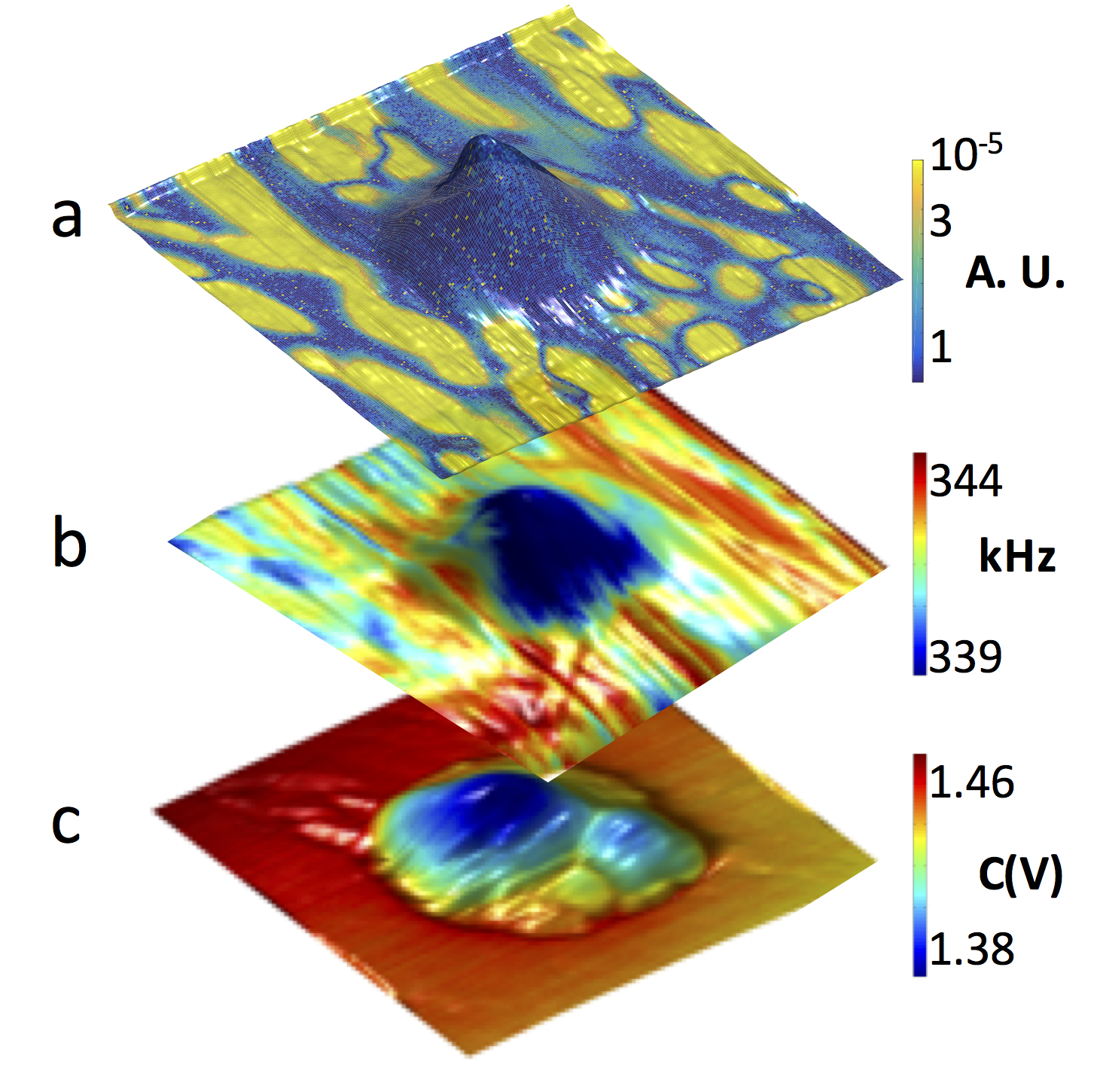
This diagram illustrates the effect of helium ions on the mechanical and electrical properties of the layered ferroelectric: a.) Disappearance domains in the exposed area; as the mound forms yellow regions (ferroelectricity) gradually disappear; b.) Mechanical properties of the material; warmer colors indicate hard areas, cool colors indicate soft areas; c.) Conductivity enhancement; warmer colors show insulating areas, cooler colors show more conductive areas.

Two-dimensional electronic devices could inch closer to their ultimate promise of low power, high efficiency and mechanical flexibility with a processing technique developed at the Department of Energy’s Oak Ridge National Laboratory.

A team led by Olga Ovchinnikova of ORNL’s Center for Nanophase Materials Sciences Division used a helium ion microscope, an atomic-scale “sandblaster,” on a layered ferroelectric surface of a bulk copper indium thiophosphate. The result, detailed in the journal ACS Applied Materials and Interfaces, is a surprising discovery of a material with tailored properties potentially useful for phones, photovoltaics, flexible electronics and screens.

“Our method opens pathways to direct-write and edit circuitry on 2-D material without the complicated current state-of-the-art multi-step lithographic processes,” Ovchinnikova said.

She and colleague Alex Belianinov noted that while the helium ion microscope is typically used to cut and shape matter, they demonstrated that it can also be used to control ferroelectric domain distribution, enhance conductivity and grow nanostructures. Their work could establish a path to replace silicon as the choice for semiconductors in some applications.

“Everyone is looking for the next material – the thing that will replace silicon for transistors,” said Belianinov, the lead author. “2-D devices stand out as having low power consumption and being easier and less expensive to fabricate without requiring harsh chemicals that are potentially harmful to the environment.”

Reducing power consumption by using 2-D-based devices could be as significant as improving battery performance. “Imagine having a phone that you don’t have to recharge but once a month,” Ovchinnikova said.

The paper, titled “Polarization control via He-ion beam induced nanofabrication in layered ferroelectric semiconductors,” is available at http://pubs.acs.org/doi/abs/10.1021/acsami.5b12056. Co-authors are Vighter Iberi, Alexander Tselev, Michael Susner, Michael McGuire, David Joy, Stephen Jesse, Adam Rondinone and Sergei Kalinin.

This research was funded through the Laboratory Directed Research and Development program. Some of the work was performed at the Center for Nanophase Materials Sciences, a DOE Office of Science User Facility.

UT-Battelle manages ORNL for the DOE’s Office of Science. The Office of Science is the single largest supporter of basic research in the physical sciences in the United States, and is working to address some of the most pressing challenges of our time. For more information, please visit http://science.energy.gov/.


Filed Under: M2M (machine to machine)


Related Articles Read More >

Part 6: IDE and other software for connectivity and IoT design work
Part 4: Edge computing and gateways proliferate for industrial machinery
Part 3: Trends in Ethernet, PoE, IO-Link, HIPERFACE, and single-cable solutions
Machine Learning for Sensors

DESIGN GUIDE LIBRARY

“motion

Enews Sign Up

Motion Control Classroom

Design World Digital Edition

cover

Browse the most current issue of Design World and back issues in an easy to use high quality format. Clip, share and download with the leading design engineering magazine today.

EDABoard the Forum for Electronics

Top global problem solving EE forum covering Microcontrollers, DSP, Networking, Analog and Digital Design, RF, Power Electronics, PCB Routing and much more

EDABoard: Forum for electronics

Sponsored Content

  • Global supply needs drive increased manufacturing footprint development
  • How to Increase Rotational Capacity for a Retaining Ring
  • Cordis high resolution electronic proportional pressure controls
  • WAGO’s custom designed interface wiring system making industrial applications easier
  • 10 Reasons to Specify Valve Manifolds
  • Case study: How a 3D-printed tool saved thousands of hours and dollars

Design World Podcasts

May 17, 2022
Another view on additive and the aerospace industry
See More >
Engineering Exchange

The Engineering Exchange is a global educational networking community for engineers.

Connect, share, and learn today »

Design World
  • Advertising
  • About us
  • Contact
  • Manage your Design World Subscription
  • Subscribe
  • Design World Digital Network
  • Engineering White Papers
  • LEAP AWARDS

Copyright © 2022 WTWH Media LLC. All Rights Reserved. The material on this site may not be reproduced, distributed, transmitted, cached or otherwise used, except with the prior written permission of WTWH Media
Privacy Policy | Advertising | About Us

Search Design World

  • Home
  • Technologies
    • 3D CAD
    • Electronics • electrical
    • Fastening & Joining
    • Factory automation
    • Linear Motion
    • Motion Control
    • Test & Measurement
    • Sensors
    • Fluid power
  • Learn
    • Ebooks / Tech Tips
    • Engineering Week
    • Future of Design Engineering
    • MC² Motion Control Classrooms
    • Podcasts
    • Videos
    • Webinars
  • LEAP AWARDS
  • Leadership
    • 2022 Voting
    • 2021 Winners
  • Design Guide Library
  • Resources
    • 3D Cad Models
      • PARTsolutions
      • TraceParts
    • Digital Issues
      • Design World
      • EE World
    • Women in Engineering
  • Supplier Listings