Design World

  • Home
  • Technologies
    • ELECTRONICS • ELECTRICAL
    • Fastening • joining
    • FLUID POWER
    • LINEAR MOTION
    • MOTION CONTROL
    • SENSORS
    • TEST & MEASUREMENT
    • Factory automation
    • Warehouse automation
    • DIGITAL TRANSFORMATION
  • Learn
    • Tech Toolboxes
    • Learning center
    • eBooks • Tech Tips
    • Podcasts
    • Videos
    • Webinars • general engineering
    • Webinars • Automated warehousing
    • Voices
  • LEAP Awards
  • 2025 Leadership
    • 2024 Winners
    • 2023 Winners
    • 2022 Winners
    • 2021 Winners
  • Design Guides
  • Resources
    • Subscribe
    • 3D Cad Models
      • PARTsolutions
      • TraceParts
    • Digital Issues
      • Design World
      • EE World
    • Educational Assets
    • Engineering diversity
    • Trends
  • Supplier Listings
  • Advertise
  • Subscribe

Robot Developed For Automated Assembly Of Designer Nanomaterials

By Institute Of Industrial Science, the University of Tokyo | April 18, 2018

A current area of intense interest in nanotechnology is van der Waals heterostructures, which are assemblies of atomically thin two-dimensional (2D) crystalline materials that display attractive conduction properties for use in advanced electronic devices.

A representative 2D semiconductor is graphene, which consists of a honeycomb lattice of carbon atoms that is just one atom thick. The development of van der Waals heterostructures has been restricted by the complicated and time-consuming manual operations required to produce them. That is, the 2D crystals typically obtained by exfoliation of a bulk material need to be manually identified, collected, and then stacked by a researcher to form a van der Waals heterostructure. Such a manual process is clearly unsuitable for industrial production of electronic devices containing van der Waals heterostructures

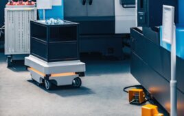
Now, a Japanese research team led by the Institute of Industrial Science at The University of Tokyo has solved this issue by developing an automated robot that greatly speeds up the collection of 2D crystals and their assembly to form van der Waals heterostructures. The robot consists of an automated high-speed optical microscope that detects crystals, the positions and parameters of which are then recorded in a computer database. Customized software is used to design heterostructures using the information in the database. The heterostructure is then assembled layer by layer by a robotic equipment directed by the designed computer algorithm. The findings were reported in Nature Communications.

“The robot can find, collect, and assemble 2D crystals in a glove box,” study first author Satoru Masubuchi says. “It can detect 400 graphene flakes an hour, which is much faster than the rate achieved by manual operations.”

When the robot was used to assemble graphene flakes into van der Waals heterostructures, it could stack up to four layers an hour with just a few minutes of human input required for each layer. The robot was used to produce a van der Waals heterostructure consisting of 29 alternating layers of graphene and hexagonal boron nitride (another common 2D semiconductor). The record layer number of a van der Waals heterostructure produced by manual operations is 13, so the robot has greatly increased our ability to access complex van der Waals heterostructures.

“A wide range of materials can be collected and assembled using our robot,” co-author Tomoki Machida explains. “This system provides the potential to fully explore van der Waals heterostructures.”

The development of this robot will greatly facilitate production of van der Waals heterostructures and their use in electronic devices, taking us a step closer to realizing devices containing atomic-level designer materials.

You Might Also Like


Filed Under: Industrial automation, Robotics • robotic grippers • end effectors


LEARNING CENTER

Design World Learning Center
“dw
EXPAND YOUR KNOWLEDGE AND STAY CONNECTED
Get the latest info on technologies, tools and strategies for Design Engineering Professionals.
Motor University

Design World Digital Edition

cover

Browse the most current issue of Design World and back issues in an easy to use high quality format. Clip, share and download with the leading design engineering magazine today.

EDABoard the Forum for Electronics

Top global problem solving EE forum covering Microcontrollers, DSP, Networking, Analog and Digital Design, RF, Power Electronics, PCB Routing and much more

EDABoard: Forum for electronics

Sponsored Content

  • Widening the scope for machine tool designers with FORTiS™ enclosed encoder
  • Sustainability, Innovation and Safety, Central to Our Approach
  • Why off-highway is the sweet spot for AC electrification technology
  • Looking to 2025: Past Success Guides Future Achievements
  • North American Companies Seek Stronger Ties with Italian OEMs
  • Adapt and Evolve
View More >>
Engineering Exchange

The Engineering Exchange is a global educational networking community for engineers.

Connect, share, and learn today »

Design World
  • About us
  • Contact
  • Manage your Design World Subscription
  • Subscribe
  • Design World Digital Network
  • Control Engineering
  • Consulting-Specifying Engineer
  • Plant Engineering
  • Engineering White Papers
  • Leap Awards

Copyright © 2025 WTWH Media LLC. All Rights Reserved. The material on this site may not be reproduced, distributed, transmitted, cached or otherwise used, except with the prior written permission of WTWH Media
Privacy Policy | Advertising | About Us

Search Design World

  • Home
  • Technologies
    • ELECTRONICS • ELECTRICAL
    • Fastening • joining
    • FLUID POWER
    • LINEAR MOTION
    • MOTION CONTROL
    • SENSORS
    • TEST & MEASUREMENT
    • Factory automation
    • Warehouse automation
    • DIGITAL TRANSFORMATION
  • Learn
    • Tech Toolboxes
    • Learning center
    • eBooks • Tech Tips
    • Podcasts
    • Videos
    • Webinars • general engineering
    • Webinars • Automated warehousing
    • Voices
  • LEAP Awards
  • 2025 Leadership
    • 2024 Winners
    • 2023 Winners
    • 2022 Winners
    • 2021 Winners
  • Design Guides
  • Resources
    • Subscribe
    • 3D Cad Models
      • PARTsolutions
      • TraceParts
    • Digital Issues
      • Design World
      • EE World
    • Educational Assets
    • Engineering diversity
    • Trends
  • Supplier Listings
  • Advertise
  • Subscribe
We use cookies to personalize content and ads, to provide social media features, and to analyze our traffic. We share information about your use of our site with our social media, advertising, and analytics partners who may combine it with other information you’ve provided to them or that they’ve collected from your use of their services. You consent to our cookies if you continue to use this website.