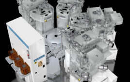
Applied Materials, Inc., through its AKT Display Business Group, announced that its AKT-55K EBT (Electron Beam Array Tester) has been selected by Samsung Electronics Corp. as the leading array test system for Samsung’s next generation TFT-LCD production line. The systems were ordered for Samsung’s new fab in Tangieong, Korea, to produce flat panels from the industry’s largest glass substrates, which will be critical to reducing the cost of large-screen LCD TVs.
“We are very pleased by Samsung’s choice of Applied Materials to supply its EBT systems as it moves to next generation TFT-LCD manufacturing,” said In Doo Kang, vice president and general manager of Applied’s AKT Display Business Group.
“Our EBT systems are being used by many flat panel manufacturers worldwide for multiple generations due to their exceptional accuracy, high throughput and low operating costs. These systems, along with our next generation PECVD and color filter sputtering systems, allow customers to reduce overall manufacturing costs by enabling the efficient production of large-size LCD TVs.”
The AKT-55K EBT system has been extensively redesigned to satisfy customers’’s largest substrate size for next generation LCD production. Seven electron beams provide rapid, accurate pixel array testing while maintaining the lowest overall operating costs. The system’s non-contact test technology enables safe testing of high-value LCD TV panels without damaging or scratching the critical display features. requirements for handling the world
Applied Materials, Inc.
www.appliedmaterials.com.
:: Design World ::
Filed Under: Semiconductor manufacture

Tell Us What You Think!