System in Package (SiP) designs reduce size and weight, sweep multiple packages from a printed wiring board (PWB) into a SiP for improved electrical performance, and reduce PWB complexity and cost.
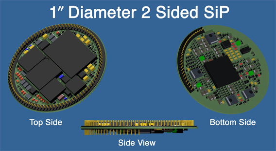
For example, a SiP conversion condensed a 7.75 x 15 in. PCB to a 2.2 x 2.2 in. size using a 3-4-3 CoreEZTM substrate with 4 signals, 6 planes, and 30 µm lw/ls; and an assembly including 5 flip chip FPGAs, CSP memory, passive components, SMT components, a PGA connector, and a 2-sided assembly.
Substrate design integration at system level is the key to getting substantial reduction in PWB design complexity and cost. Elements include organic substrates for significant weight reduction (Thin PTFE substrates are typically 1/10 the weight of a comparable ceramic substrate); thin substrates for significant electrical performance improvements; SiP designs for shorter signal paths; and pinned or BGA PWB interfaces.
Endicott Interconnect Technologies, Inc.
www.eitny.com
: Design World :
Filed Under: Semiconductor manufacture, ELECTRONICS • ELECTRICAL

Tell Us What You Think!