Design World

  • Home
  • Technologies
    • 3D CAD
    • Electronics • electrical
    • Fastening & Joining
    • Factory automation
    • Linear Motion
    • Motion Control
    • Test & Measurement
    • Sensors
    • Fluid power
  • Learn
    • Ebooks / Tech Tips
    • Engineering Week
    • Future of Design Engineering
    • MC² Motion Control Classrooms
    • Podcasts
    • Videos
    • Webinars
  • LEAP AWARDS
  • Leadership
    • 2022 Voting
    • 2021 Winners
  • Design Guide Library
  • Resources
    • 3D Cad Models
      • PARTsolutions
      • TraceParts
    • Digital Issues
      • Design World
      • EE World
    • Women in Engineering
  • Supplier Listings

Technology Reduces 30 Percent Chip Area of STT-MRAM While Increasing Memory Bit Yield By 70 Percent

By Tohoku University | May 17, 2016

Share

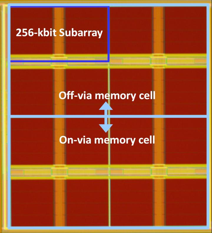
Fabricated 2-Mbit MRAM test chip for verifying the developed MTJ formation technology directly on via hole in VLSI. Credit Yoichi Oshima

In a world first, researchers from Tohoku University have successfully developed a technology to stack magnetic tunnel junctions (MTJ) directly on the vertical interconnect access (via) without causing deterioration to its electric/magnetic characteristics. The via in an integrated circuit design is a small opening that allows a conductive connection between the different layers of a semiconductor device.

This new discovery will be particularly significant in reducing the chip area of spin-transfer torque magnetic random access memory (STT-MRAM), making its commercialization more practical.

The team led by Professor Tetsuo Endoh, Director of the Center for Innovative Integrated Electronic Systems (CIES), focused on reducing the memory cell area of STT-MRAMs in order to lower manufacturing costs, making them competitive with conventional semiconductor memories like dynamic random access memory (DRAM).

Because MTJs use magnetic properties, the quality of the surface between the MTJ and its lower electrode is important. If the surface area is not smooth, the electric/magnetic characteristics of the MTJ will degrade. For this reason, placing an MTJ directly on the via holes in STT-MRAMs has been avoided until now, although it increases the size of the memory cell.

Endoh’s group has tackled the issue by developing a special polishing process technology to prevent any interference between the MTJ and its lower electrode. The technology’s effectiveness was successfully verified by an experiment using single-MTJ test chips.

To further test the success of this development, a 2-Mbit STT-MRAM test chip integrating the new technology has been designed to verify the space needed for the integrated circuits – this includes more than 1million MTJs.

“Not only does this test chip show a 70% improvement in its memory bit yield compared to standard STT-MRAM, but its memory cell area is reduced by 30%,” says Endoh. “It will be very effective for reducing the chip area of MRAM.”

CIES develops material, process, circuit and test technologies in integrated electronic systems. The center’s main focus is on developing high-performance, low-power technologies for a more energy-efficient society.

The results of this research were presented at the IEEE International Memory Workshop in France on May 16, 2016.
This research was supported by the CIES consortium project.


Filed Under: Industrial automation


Related Articles Read More >

Festo and the power of worker upskilling at the Oracle Industry Lab
Five ways to drive ROI from personnel and cobot investments
Safety Air Guns use engineered air nozzles for high performance
EXAIR’s new no drip siphon fed spray nozzle coats, cools and cleans

DESIGN GUIDE LIBRARY

“motion

Enews Sign Up

Motion Control Classroom

Design World Digital Edition

cover

Browse the most current issue of Design World and back issues in an easy to use high quality format. Clip, share and download with the leading design engineering magazine today.

EDABoard the Forum for Electronics

Top global problem solving EE forum covering Microcontrollers, DSP, Networking, Analog and Digital Design, RF, Power Electronics, PCB Routing and much more

EDABoard: Forum for electronics

Sponsored Content

  • Renishaw next-generation FORTiS™ enclosed linear encoders offer enhanced metrology and reliability for machine tools
  • WAGO’s smartDESIGNER Online Provides Seamless Progression for Projects
  • Epoxy Certified for UL 1203 Standard
  • The Importance of Industrial Cable Resistance to Chemicals and Oils
  • Optimize, streamline and increase production capacity with pallet-handling conveyor systems
  • Global supply needs drive increased manufacturing footprint development

Design World Podcasts

June 12, 2022
How to avoid over engineering a part
See More >
Engineering Exchange

The Engineering Exchange is a global educational networking community for engineers.

Connect, share, and learn today »

Design World
  • Advertising
  • About us
  • Contact
  • Manage your Design World Subscription
  • Subscribe
  • Design World Digital Network
  • Engineering White Papers
  • LEAP AWARDS

Copyright © 2022 WTWH Media LLC. All Rights Reserved. The material on this site may not be reproduced, distributed, transmitted, cached or otherwise used, except with the prior written permission of WTWH Media
Privacy Policy | Advertising | About Us

Search Design World

  • Home
  • Technologies
    • 3D CAD
    • Electronics • electrical
    • Fastening & Joining
    • Factory automation
    • Linear Motion
    • Motion Control
    • Test & Measurement
    • Sensors
    • Fluid power
  • Learn
    • Ebooks / Tech Tips
    • Engineering Week
    • Future of Design Engineering
    • MC² Motion Control Classrooms
    • Podcasts
    • Videos
    • Webinars
  • LEAP AWARDS
  • Leadership
    • 2022 Voting
    • 2021 Winners
  • Design Guide Library
  • Resources
    • 3D Cad Models
      • PARTsolutions
      • TraceParts
    • Digital Issues
      • Design World
      • EE World
    • Women in Engineering
  • Supplier Listings