by JAMES COLBY, Littelfuse
Circuit protection technologies and board layout strategies help promote safety, reliability and connectivity.
There’s one down-side to wearable technology that is unlikely to show up in headlines about the IoT: Human bodies generate static electricity as they move. That static electricity can potentially harm the sensitive electronics that power IoT applications.
To understand the problem, consider the human-body model (HBM), a model used for characterizing the susceptibility of integrated circuits to damage from electrostatic discharge (ESD). The most widely used HBM definition is the test model defined in the military standard MIL-STD-883, Method 3015.8, Electrostatic Discharge Sensitivity Classification. A similar international HBM standard is JEDEC JS-001. In both JS-001-2012 and MIL-STD-883H, the charged human body is modeled by a 100-pF capacitor and a 1.5-kΩ discharging resistor. During testing, the capacitor is fully charged in a range between 250 V and 8 kV, then discharged through the 1.5-kΩ resistor in series to the device under test.
Because wearables are designed to be worn next to the skin, they are constantly bombarded by static electricity generated by close interaction with the user. Without proper protection, the device’s sensor circuits, battery-charging interfaces, buttons or data I/Os could be damaged by ESD levels similar to those generated in the HBM tests. If the wearable device fails, the functions and reliability of the overall network can degrade.
Advanced circuit protection technologies and board layout strategies can safeguard wearable devices and their users. Applying these recommendations early in the design process will help circuit designers improve the performance, safety and reliability of their wearable technology designs and help build a more reliable IoT.
Big ESD protection, small package
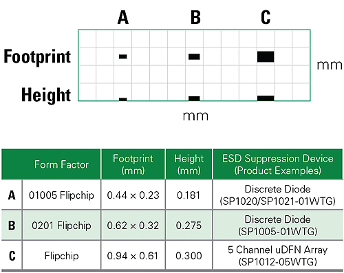
One problem with designing protection for wearable circuits is that wearable electronics are small and getting smaller. In the past, it took large diode structures in large packages (for example, 0603 [with a footprint of about 1.6 × 0.81 mm] and 0402 [about 1.0 × 0.8601-mm footprint]) to protect against ESD and realize low clamping voltages. But there have been steady improvements in wafer fabrication processes and back-end assemblies that now make it possible to get serious ESD protection in a small form factor. For example, consider the general-purpose 01005 transient voltage suppression (TVS) diode from Littelfuse. It sits in a package having an outline measuring 0.45 × 0.24 mm and can withstand 30 kV contact discharge (IEC 61000-4-2). It also has a dynamic resistance value of less than 1 Ω.
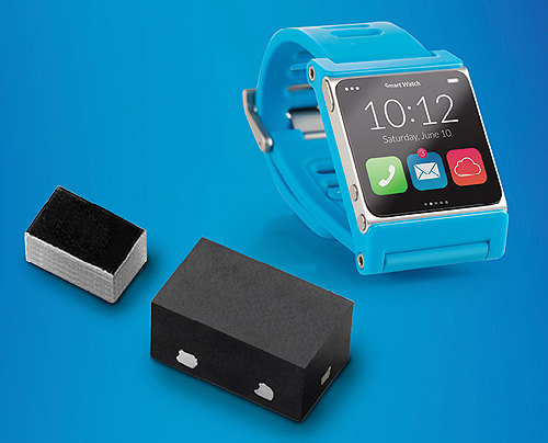
To see why robust ESD protection is important, again consider the HBM. It specifies test levels beginning at 250 V, but most application designers ensure their equipment meets at least Level 4 of the IEC 61000-4-2 test standard (8 kV contact, 15 kV air discharge). In many portable devices and wearables, the contact discharge design level is being raised to 15 or 20 kV, with some companies setting it as high as 30 kV. Compact ESD devices are robust enough to meet these demanding conditions.
Use of modern ESD technologies can save a lot of circuit board space. For example, the most common discrete form factor for TVS diodes is the SOD882 package, which has an outline of 1.0 × 0.6 mm. Moving to a device having a 0201 form factor (0.6 × 0.3 mm) takes up only 30% of the board area. Furthermore, a device having a 01005 outline (0.4 × 0.2 mm) brings an 85% space savings compared to the SOD882 package.
Despite their small outline, today’s TVS diode devices perform well without compromising ESD protection. In fact, discrete semiconductors with a small form factor can have the same level of ESD protection (30 kV contact discharge) and clamping performance (dynamic resistance < 1 Ω) as their larger counterparts (for example, SOD323 and SOD123). However, the small size of the component may present manufacturing challenges. At 0.4 × 0.2 mm, the 01005 package will need well-designed board treatments, such as solder pads and thick stencils, to ensure the component does not slide or “tombstone” during the reflow solder process.
Selection and configuration
A few key points about the selection and configuration of TVS diode technologies will help design engineers optimize their wearable designs.
Know when to choose unidirectional versus bidirectional diodes. TVS diodes come in unidirectional or bidirectional (back-to-back) configurations. Unidirectional diodes are typically used for dc circuits, including pushbuttons and switches, as well as digital circuits (low-voltage differential signaling). Bidirectional diodes are used in ac circuits, which may include any signal with a negative component greater than -0.7 V. These circuits include audio, analog video, legacy data ports and RF interfaces.
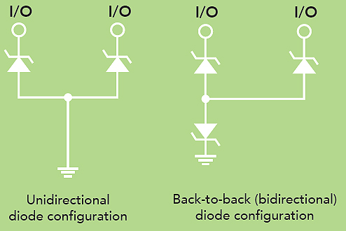
Whenever possible, design engineers should choose unidirectional diode configurations because they perform better during negative-voltage ESD events. During these discharges, the clamping voltage will be based on the forward bias voltage of the diode, which is typically less than 1.0 V. In contrast, a bidirectional diode configuration provides a clamping voltage during a negative strike that is based on the reverse breakdown voltage, which is higher than the forward bias of the unidirectional diode. Thus, the unidirectional configuration can dramatically reduce the stress on the system during negative strikes.
Position diodes judiciously. Most wearable designs do not need TVS diodes on the PCB at each integrated circuit pin. Instead, the designer should determine which pins have exposure to the outside of the application where user-generated ESD events are likely. If the user can touch a communication/control line, it could become a path for ESD to enter the integrated circuit. Typical circuits prone to compromise this way include USB, audio, button/switch control and other signal lines. Adding these discrete protection devices will take up board space, so it is important to get devices that fit in small 0201 or 01005 outlines. For some wearable applications, space-saving multi-channel arrays are available. Regardless of package style, the ESD suppressor should sit as close as possible to the ESD source. For example, protection for a USB port should sit close to the USB connector.
Keep traces short. Trace routing is important in the design of TVS diode protection for integrated circuit pins. Unlike lightning transients, ESD does not unleash a large amount of current for long durations. To handle ESD, it is important to move the charge from the protected circuit to the ESD reference as quickly as possible.
The length of the trace—from the signal line to the ESD component and from the ESD component to ground—is the overriding factor, not the width of the trace to ground. The trace length should be as short as possible to limit parasitic inductance. This inductance will result in inductive overshoot, which is a brief voltage spike that can reach hundreds of volts if the stub trace is long enough. Recent package developments include µDFN outlines that fit directly over the data lanes to eliminate the need for stub traces.
Understand HBM, Machine Model (MM) and Charged Device Model (CDM) definitions. In addition to HBM, MM and CDM are test models for characterizing how well ICs running the portable device or wearable withstand ESD. Many semiconductor makers consider MM to be obsolete. It tends to track HBM in terms of robustness and in failure modes produced, though some producers still employ it. CDM is another alternative to the HBM. Instead of simulating the interaction between a human and an IC, the CDM simulates an IC sliding down a track or tube, then touching a grounded surface. Devices classified according to CDM are exposed to a charge at a given voltage level, then tested for survival. If the device still functions, it is tested at the next level and so on, until failure. CDM is standardized by JEDEC in JESD22-C101E.

Chips that include the processor, memory and ASIC would all be characterized with one or more of these models. Semiconductor suppliers use the models to ensure the robustness of the circuits during manufacturing. The current trend is for suppliers to reduce the voltage test levels because doing so saves die space and because most suppliers adhere to excellent in-house ESD policies.
Strict ESD policies benefit the supplier by allowing for lower on-chip ESD protection, but circuit designers end up with a chip that is sensitive to application-level ESD and which must be prevented from failing due to field-level or user-induced ESD. Designers must select a protective device able to protect against intensifying electrical stresses while clamping voltages low enough to protect the highly sensitive integrated circuitry.
When evaluating ESD protection devices, consider the following parameters:
1. Dynamic resistance: This value is a measure of how well the diode will clamp and divert the ESD transient to ground. It helps determine how low the resistance of the diode will be after it switches on. The lower the dynamic resistance, the better.
2. IEC 61000-4-2 rating: The TVS diode supplier determines this value by increasing the ESD voltage until the diode fails. The failure point characterizes the robustness of the diode. For this parameter, the higher the value, the better. A growing number of Littelfuse TVS diodes can reach as high as 20 and 30 kV contact discharge, which far exceeds the highest level of the IEC 61000-4-2 (Level 4 = 8 kV contact discharge).
As the wearable market continues to grow, so too does the need for circuit protection. In fact, it is more important than ever to consider ESD protection and proper board layout practices early in the design process. Circuit protection devices, such as TVS diodes, can help protect the sensitive integrated circuitry inside wearable devices to maintain the value proposition of the IoT ecosystem.
References
Littelfuse
www.littelfuse.com
![]()
Filed Under: Wireless • 5G and more, Power Electronic Tips


