Switching regulators are smaller and more efficient than linear regulators, but linear regulators are simpler and quieter. The application’s specific requirements determine the final choice.
As electronic products become more sophisticated and pack new features into smaller housings, they need more efficient power supplies with higher power density and lower heat dissipation. In addition, ac power supplies and battery charging devices need to be isolated from the ac line and have efficient voltage regulators, while battery charging circuits need to extend time between recharges and shorten charging times. To satisfy these requirements and make power supply design easier and faster, most semiconductor device manufacturers have kept pace with the demand and offer sophisticated, low-cost devices for small, efficient, high-power-density power supplies.
Linear power supplies
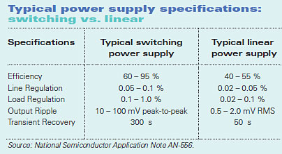
Most small and medium-duty power supplies intended for consumer, medical, and light industrial uses come in two basic types, either linear or switching configurations. Linear power supplies are relatively simple, have excellent load and line regulation with low output ripple, and emit low levels of EMI. They also respond quickly to load and line fluctuations and require few external components. The simplest configuration needs only a regulator IC and two capacitors: one on the input, and one on the output. A major disadvantage, however, is its relatively low power density and efficiency.
Efficiency: A linear regulator’s power loss comes from the way in which it maintains a constant output voltage. A linear regulator drops a voltage that is equal to the difference between the input and output voltages: Vdo = Vin – Vout . Because the output current passes through both the load and the regulator, the power dissipated by the regulator is Pr = Vdo Io:
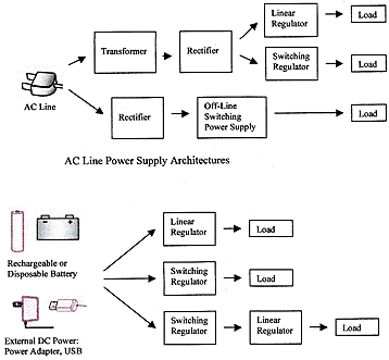
AC line, external power adapters, batteries, and USB ports are the most common sources of electric power for today’s electronic devices.
Where:
Vin = input voltage
Vout = output voltage
Vdo = dropout voltage
Io = output current
Pr = power dissipated by regulator
Efficiency is critical because wasted power shortens operating time for battery-powered devices and creates heat, which must be removed with a heat sink or a cooling fan. For example, in a classical automotive 5V voltage regulator, more power is dissipated as heat than is used to power the load. The charging system typically generates 14.3V, and the voltage dropped by the regulator to maintain constant output is Vdo = 14.3V — 5.0V = 9.3V. If the load current is 1.0A, for example, the power delivered to the load is 5W, but the power dissipated by the linear regulator is 9.3W.
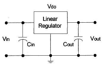
The simplest 3-lead voltage regulator IC needs only two additional capacitors for stable operation.
Power supply efficiency deals with the input power, power delivered to the load, and power dissipated by the regulator. It can be expressed as a ratio of the output power Pout to input power Pin. Neglecting the regulator ground pin current (assume Iin = Io), the approximate efficiency is:
E = Pout/ Pin ,
E = Io Vout / IinVin , or
E = Vout / Vin.
For the example, efficiency E = 5/14.3 = 35%.
Of course, lowering the minimum input voltage improves the efficiency, but it should never go below the minimum determined by the load voltage and the regulator dropout voltage. Traditional linear voltage regulators typically use NPN-Darlington transistors for series pass components and have a minimum dropout voltage Vdo of 2.0V. The input and output voltages will have at least a 2-V difference, which limits the efficiency, especially if the output voltage is low. Also, depending on the application and the selected linear regulator, the ground pin (or no-load) current adds to the power losses.
Low-dropout: To increase efficiency and overcome the dropout limitation of conventional voltage regulators, low-dropout (LDO) regulators use PNP or CMOS power transistors. The typical dropout voltage is 200mV for PNP-based LDOs and 50mV for CMOS devices.
Many newer LDOs have extremely low quiescent current, which can be neglected. Then, to calculate efficiency:
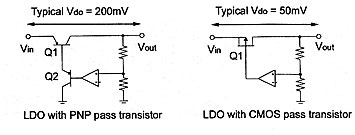
By using PNP bi-polar or CMOS pass transistors, LDOs drastically reduce the dropout voltage. Low dropout voltage is an advantage in battery powered equipment when maintaining regulation while the battery is discharging almost down to the regulated voltage. It lengthens the discharge time of the battery and increases overall efficiency of the power supply.
E = Vout / Vin
Similar to a conventional linear regulator, the minimum input LDO voltage should be greater than Vin = Vout + Vdo. Because the Vdo is so low, the LDO efficiency can be quite high.
Consider a power supply for portable battery powered equipment which uses an LDO linear regulator. A Lithium-ion 3.3V battery is its power source, the desired regulated load voltage is 2.5V, and the maximum load current is 1.0A.
For a voltage regulator, select the Texas Instruments TPS796xx LDO family, which is optimized for extremely low noise of only 40µV rms. It is suitable for audio, RF, BluetoothTM, PDA, cell phone, and other portable equipment applications. The output voltage range is 1.225 to 5.5-Vdo and the maximum current is 1.0 A. Its dropout voltage is only 250mV at full load with a typical ground-pin current of 265 µA.
The output voltage is designated by the last two digits of the regulator part number, so for 2.5V select the TPS79625 device. Ignore battery internal resistance, and consider the initial battery discharge voltage to be 3.9V. The low dropout voltage allows almost 100% of available battery capacity to be used, so the battery cut-off voltage is set at 3.0V.
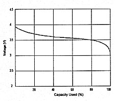
Most Li-ion batteries use a graphite negative electrode. They have a relatively flat discharge voltage curve and should be discharged to 3.0V per cell.
With a fully charged battery, the regulator efficiency is:
E = 2.5/3.9 = 0.64 (64%).
When the battery is almost completely discharged, the efficiency is:
E = 2.5/3.0 = 0.83 (83%).
Although LDOs are capable of extremely high efficiency, the input and output voltages must be extremely close. In some cases, a step-down switching regulator is followed by an LDO linear regulator to achieve overall higher efficiency, load regulation, and faster response.
Switching power supplies
Compared to linear technology, switching power supplies have higher efficiencies, lower heat dissipation, and higher power density. But line and load regulation are not as good as linear regulators, and due to their switching operation, they produce higher levels of EMI. They are also more complex than the linear regulators and require an inductor, which many designers typically dislike. Because these regulators convert voltage from one level to another, they are often called converters.
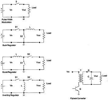
Although other variations are available, Buck, Boost, Inverting, and Flyback topologies are the most commonly used switching regulators.
Switching voltage regulators come in various topologies, which include pulse-width modulation (PWM), Buck, Boost, Buck-Boost, and Flyback. Some convert the voltage, such as a Boost or reverse-polarity power supply.
PWM/Buck: The oldest method, pulse-width modulation (PWM), controls the average load voltage by changing the duty cycle while operating at a fixed frequency. By comparison, Buck dc-dc converters, also called step-down switching regulators, use an inductor connected on the output side to average the voltage. The output voltage is lower than the input voltage and has the same polarity.
Boost: The output voltage of a Boost or step-up converter is greater than the input voltage and has the same polarity. The inductor in this case is connected to the input terminal and is constantly switched between the ground and the load. Without a transformer, only switching power supplies are capable of increasing dc voltage.
Buck-Boost: When the inductor is connected to ground and switched alternately between the input and output, the voltage polarity inverts and can be used to maintain the voltage magnitude higher or lower than the input voltage. Such converters are called Buck-Boost or inverting switching regulators. Only switching power supplies can change polarity and magnitude of the dc voltage.
Flyback: A Flyback converter is the main element of an off-line switching supply. This type of power supply needs only a rectifier at the front end to connect directly to the 110V/220V line. The inductor is replaced with a high-frequency transformer to electrically isolate it. Because of its high switching frequency, the transformer is much smaller and lighter than a 50/60Hz transformer. This type of power supply is commonly used in desktop computers and other office equipment.
A practical switching regulator circuit, at a minimum, requires an input capacitor to maintain a steady input voltage, an output capacitor to filter the ripple current and maintain the dc voltage, a diode to replace one of the switches, and a switching regulator IC with an internal or external switching transistor.
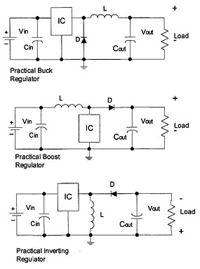
The simplest practical Buck, Boost, and Inverting switching power supplies consist of a regulator IC, input and output capacitors, an inductor, and a rectifier diode.
With the exception of the Flyback circuit, the first three topologies operate in a similar fashion by storing energy first in the inductor L and then transferring it to the output capacitor Cout. Either an external pass transistor or an internal transistor of the switching voltage regulator IC turns on and off by the controller circuitry to maintain the preset voltage across the load. In the boost circuit the ultra-fast rectifier D quickly charges Cout and blocks the current from flowing back into the regulator. In the buck regulator, D, L, and Cout provide a path for current to free wheel after the pass transistor turns off.
Modern switching power supplies operate at frequencies in hundreds of kHz and even several MHz. Because higher switching frequencies require lower values of capacitors and inductors, their sizes can be reduced to a fraction of those required at 50/60Hz. For example, the LTC3602 step-down switching regulator recently released by Linear Technology claims efficiency over 90% and can be programmed to run at up to 3MHz. At 1MHz and an output of 3.3V at 2.5A, the required inductor and output capacitor are only a 2.2µH and 100µF.
Fine-tuned for boosting 5V to 12V at 700 mA, National Semiconductor’s LM2735 Integrated Switch Step-up switching regulator operates at 1.6 MHz, is internally compensated, and requires only a few small passive components. Because of its high switching frequency, the output capacitor is only 10µF and the inductor is 15µH.
Some regulator ICs require an external pass transistor (switch), while others have an integrated switch. Typically, integrated switch converters yield the highest efficiency and smallest size. For high power conversion, semiconductor manufacturers offer high-efficiency external switches designed for specific converter topologies. For example, the high-power FDMS9600S integrated MOSFET Module from Fairchild Semiconductor incorporates not only high side and low side MOSFETs, but also an integrated Schottky diode for maximum efficiency. A buck regulator using this external switch, a controller, driver, inductor, and capacitor can supply 14A with a maximum efficiency of 90% at 6A.
Switching regulator efficiency depends on the topology, input and output voltage, load current, and proper selection of all components. To find the sources of power losses in switching regulators, consider the following practical boost regulator, which contains an internal pass switching transistor.
The forward voltage drop across the diode D becomes significant when the output voltage is below 10V. Even Schottky rectifiers have a forward voltage drop of approximately 0.5V, so at Vout = 5V, 10% of power is lost across the rectifier diode.
The internal or external switching transistor (bi-polar or MOSFET) creates a voltage drop in the saturated state, plus switching losses when the transistor crosses over into the active state. In addition, driver circuitry required to control the pass transistor consumes some power.
When properly selected, capacitors Cin and Cout dissipate low power, which can be determined as follows: Capacitor Losses = ESR I2RMS , where ESR is the capacitor’s Effective Series Resistance and I2RMS is the square of RMS current. The inductor L has resistive losses due to the resistance of the copper wire winding and core losses that depend on core material, voltage, and other design factors. In buck-type switching regulators, the power transistor and the Schottky diode are also the main sources of power losses that become more significant when lower output voltage is needed.
In all switching topologies, faster MOSFETs are often used instead of slower bi-polar transistors. However, frequencies higher than the optimum increase MOSFET losses, which mainly occur when the transistor is in the active state during the on-off or off-on transition. Extremely low voltage drop across the MOSFET transistor compared to the bi-polar device is another reason for its higher efficiency.
The common 5V supply bus that originated with TTL logic has long been the most widely used regulated voltage. The switching power supply efficiency at 5V and above is superior to that of linear power supplies. The newer 3.3V standard voltage, which replaces the 5V bus, brings the efficiency of the switching and the LDO power supplies closer together. As new devices operate at even lower voltages, switching power supplies lose their efficiency edge and new LDOs that require considerably less filtering and produce low noise might be the better choice for new designs.
Texas Instruments
www.ti.com
National Semiconductor
www.national.com
Linear Technology
www.linear.com
STMicroelectronics
www.st.com
Fairchild Semiconductor
www.fairchildsemi.com
Filed Under: Semiconductor manufacture, Power supplies

Tell Us What You Think!