Laser direct structuring (LDS) is the first step of a manufacturing process that creates circuit traces on molded thermoplastic components. Currently the leading technology for producing cell-phone antennas, LDS has also been widely employed to manufacture a range of components for use in medical devices, security shields, automotive sensors, and GPS antennas — anywhere product miniaturization requires embedding circuits onto a molded component of a device.
The LDS process utilizes a laser tool to lay a pattern onto a two- or three-dimensional object that will be the foundation for subsequent metallization. Artwork from a CAD file is translated into laser plotting software. Structuring occurs when the laser tool activates metal organic additives in the (LDS Grade) plastic part. This allows the electroless plating to attach to the structured areas only.
At SelectConnect Technologies, we conducted an experiment to determine exactly how close LDS traces can be structured and metalized without inducing over plating or bridging on PET/PBT material. Trace widths of 0.010 in (0.254 mm) with a spacing of 0.010 in (0.254 mm) have been successfully created. This report will determine the feasibility of trace widths and spacing below these dimensions.
We designed a geometric pattern with varying trace widths and spacing distances and structured it onto plaques made from PET/PBT. Following this, the plaques were plated with copper, nickel, and immersion gold. The patterns were examined for signs of over plating. Trace widths and spacing distances were measured using video microscopy equipment.
Method
This section provides commentary for several essential elements needed for producing LDS MIDs: CAD file guidelines, the structuring process, the plating process, the measuring equipment used, and any process variables/influences.
- CAD Files
The artwork to be structured must be generated by CAD software using certain guidelines. Generally, Pro-E or Solid Works work very well because files can be created in either STEP or IGES formats. However, the final file used for fabricating the laser program must be in STEP format.
Virtually any type of geometry can be structured. One important design guideline is all geometry or artwork must be a surface that has a zero height (Z=0 in.). This ensures that the artwork will be processed properly by the Microline laser system software. In addition, all modeled surfaces must be continuous. If there are any breaks or discontinuities, these will be reflected in the final structured product.
- Overview of the Structuring Process
Once the laser machine is setup with a robust program, it can now structure the artwork onto the plastic part. It is important for the part to be held firmly by a fixture. This will help the laser’s camera system to identify the alignment points more quickly. Once the alignment points are found, structuring occurs.
- The Plating Process
Stringent operating procedures must be followed to ensure that the LDS components are plated properly. Part handling and racking, cleaning/pre-treatment, plating bath concentrations, and temperatures, as well as the amount of time the parts are spent immersed in the solutions are a few of the critical process areas that must be carefully considered, planned for, and followed.
Standard plating thicknesses include: copper (Cu) 250 µin. (0.00635 mm), nickel (Ni) 120 µin. (0.00305mm), and immersion gold (Au) ~4-10 µin. (0.0001-0.00025 mm).
- Measuring Equipment Used
It is important to accurately measure the width of the traces and the spacing distances. The goal is to discover how narrow the traces can be at the closest spacing possible without the plating bridging or shorting.
The measuring device used is a Scienscope MZ7-PK5-FR-U Dual Arm stand microscope. It can successfully measure distances in inches through 4 decimal places reliably. Inspection is accomplished through an integrated video system. Once an object is in the lens’ field of view, the image is projected onto a computer monitor. From here one can measure the distance using the microscope’s included software.
- Process Variables/Influences
- Materials
There are a variety of materials suitable for the LDS process. The following list was taken from the LPKF LDS-MID Design Guide Ver. 2.1:
|
LCP |
PA 6/6T |
PBT |
PBT/PET |
|
PPA |
PC |
PC/ABS |
The three most common types are LCP, PC/ABS, and PBT/PET, our focus for this article. When a part is molded, it is important that it is designed properly in order to reduce knit lines or surface roughness. Structuring over extremely rough surface finishes can produce unreliable plating results.
- Laser Optimization
There are three primary laser settings that are required for successful laser structuring. They are power (watts), frequency (kHz), and speed (mm/s). The settings are unique for each LDS material type. LPKF has conducted in depth research in this area and prepared tables with the appropriate settings for each material type. Slight modifications to these recommended values are acceptable if structuring and plating integrity are improved as a result.
Results
A simulated circuit pattern was structured onto two PET/PBT plaques. Distance measurements were taken in three areas on the plaque.
|
Trace Spacing Plaque A (in.) |
Trace Line Width Plaque A (in.) |
Trace Spacing Plaque B (in.) |
Trace Line Width Plaque B (in.) |
Element Spacing Plaque A (in.) |
Element Spacing Plaque B (in.) |
|
0.0021 |
0.0060 |
0.0028 |
0.0060 |
0.0088 |
0.0084 |
|
0.0025 |
0.0063 |
0.0025 |
0.0056 |
0.0077 |
0.0081 |
|
0.0025 |
0.0060 |
0.0021 |
0.0056 |
0.0077 |
0.0081 |
|
0.0025 |
0.0056 |
0.0025 |
0.0067 |
0.0081 |
0.0081 |
|
0.0023 |
0.0056 |
0.0025 |
0.0060 |
0.0081 |
0.0088 |
|
Avg = 0.0024 |
Avg = 0.0059 |
Avg = 0.0025 |
Avg = 0.0060 |
Avg = 0.0081 |
Avg = 0.0083 |
Table 1: Trace Spacing and Widths as measured on 2 PET/PBT Plaques.
From table 1, one may observe several things. The first is that the trace spacing for both plaques ranged from 0.0021 in. (0.0533 mm) to 0.0028 in. (0.0711 mm). This is significantly closer than the current production capabilities of 0.010 in. (0.0254 mm). Next, the trace line widths varied from 0.0056 in. (0.1422 mm) to 0.0067 in. (0.1702 mm). This achievement is dramatically narrower than 0.010 in. (0.0254 mm), the present production width. Finally, the element spacing fell within 0.0077 in. (0.1956 mm) to 0.0088 (0.2235 mm). This is closer than what has been in production previously. In theory, it is possible that spacing could be tightened up further.
Discussion
Figure 1 on the next page illustrates what the simulated circuit pattern looks like. It is comprised of many elements spaced closely together connected by several conductor paths or traces. The exploded view defines the trace spacing, trace line width, and element spacing mentioned in Table 1.
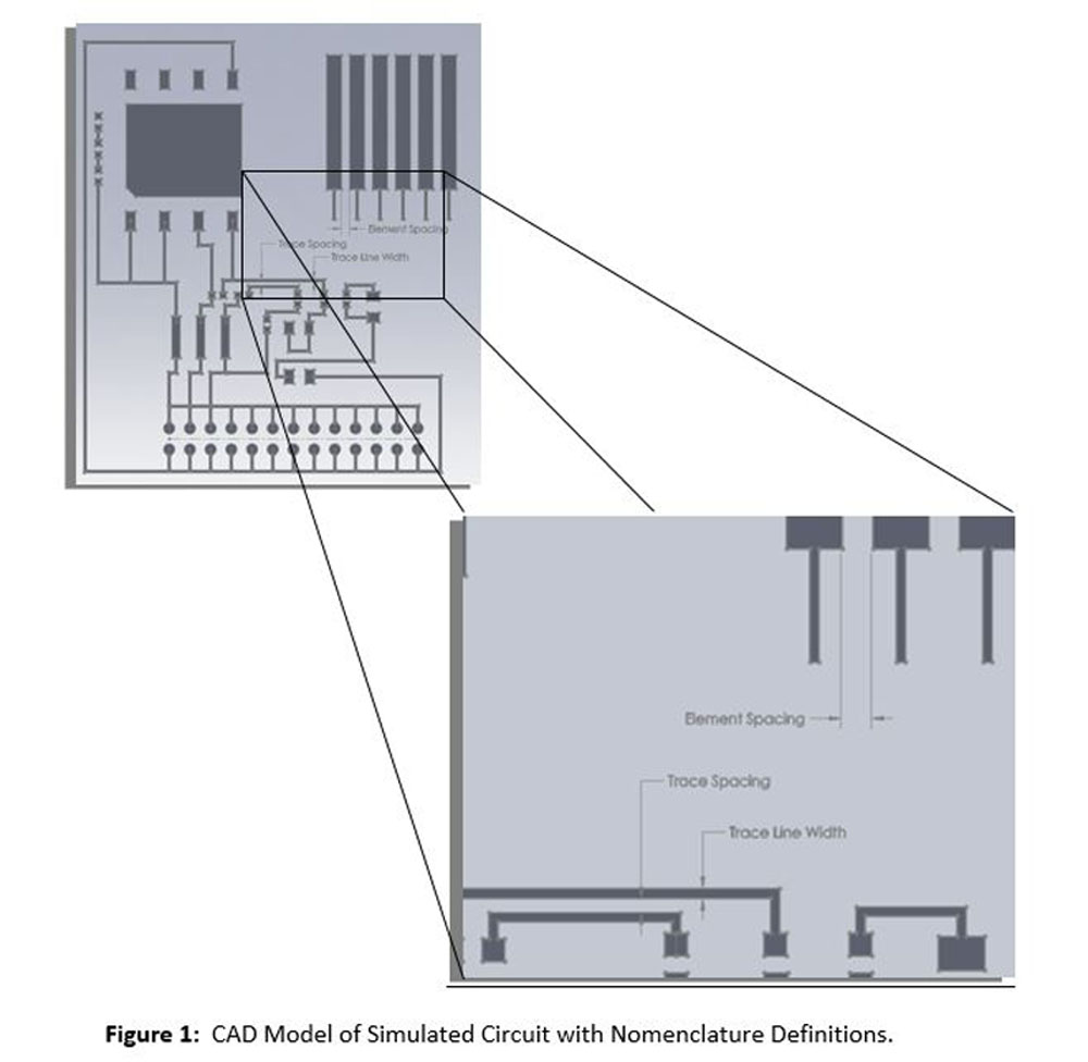
Figure 1 was modeled using Solid Works. It was done by making one closed sketch. This sketch was converted to zero height (Z=0 in.) surfaces. With the surfaces complete, the file can be saved as a STEP file for importation into the LPKF Microline 160 software for further processing.
After laser processing, the two plaques were plated using the plating process described in the Method section. They were plated to the standard thicknesses: copper (Cu) 250 µin. (0.00635 mm), nickel (Ni) 120 µin. (0.00305mm), and immersion gold (Au) ~4-10 µin. (0.0001-0.00025 mm). The plating turned out very well for these plaques. This can be partially attributed to the surface roughness of the plaques being minimal and without knit lines. There was no evidence of over-plating or extraneous plating in undesired areas. The plated artwork appeared crisp and well-defined.
Table 1 in the Results sections shows the values from the measurements taken for both plaques. Five measurements were taken by the Scienscope MZ7-PK5-FR-U microscope at each area of interest for each plaque. For all three locations, successful plating was achieved with widths and spacing below the current production value of 0.010 in. (0.0254 mm). Trace spacing as low as 0.0021 in. (0.0533 mm) and trace widths as low as 0.0056 in. (0.1422 mm) were generated.
Conclusion
In summary, the PET/PBT plaques plated very well. The absence of knit lines and surface defects contributed to continuous plating coverage over the structured areas. It was feasible to plate traces and elements with spacing and trace widths well below the current production standards of 0.010 in. (0.0254 mm). Success is attributed to correct laser program settings, parts handling, and robust plating processes.
For further information, please contact [email protected].
Filed Under: Rapid prototyping