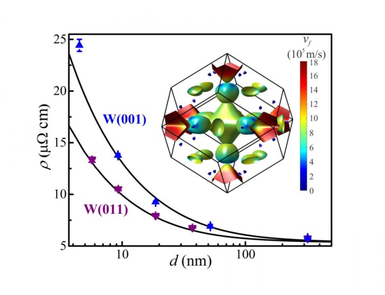
The measured resistivity of epitaxial tungsten layers with (001) and (011) crystal orientation vs thickness d. The tungsten Fermi surface is color coded according to the wave vector dependent Fermi velocity vf. At small thickness, where surface scattering dominates, W(011) is nearly twice as conductive as W(001). Transport simulations indicate that this is due to the anisotropy in the Fermi surface. These results indicate how narrow wires in future computer chips can be made two times more conductive, effectively reducing the required electric power by 50 percent. Image credit: Daniel Gall, Rensselaer Polytechnic Institute
As microchips become ever smaller and therefore faster, the shrinking size of their copper interconnects leads to increased electrical resistivity at the nanoscale. Finding a solution to this impending technical bottleneck is a major problem for the semiconductor industry.
One promising possibility involves reducing the resistivity size effect by altering the crystalline orientation of interconnect materials. A pair of researchers from Rensselaer Polytechnic Institute conducted electron transport measurements in epitaxial single-crystal layers of tungsten (W) as one such potential interconnect solution. They performed first-principles simulations, finding a definite orientation-dependent effect. The anisotropic resistivity effect they found was most marked between layers with two particular orientations of the lattice structure, namely W(001) and W(110). The work is published this week in the Journal of Applied Physics, from AIP Publishing.
Author Pengyuan Zheng noted that both the 2013 and 2015 International Technology Roadmap for Semiconductors (ITRS) called for new materials to replace copper as interconnect material to limit resistance increase at reduced scale and minimize both power consumption and signal delay.
In their study, Zheng and co-author Daniel Gall chose tungsten because of its asymmetric Fermi surface — its electron energy structure. This made it a good candidate to demonstrate the anisotropic resistivity effect at the small scales of interest. “The bulk material is completely isotropic, so the resistivity is the same in all directions,” Gall said. “But if we have thin films, then the resistivity varies considerably.”
To test the most promising orientations, the researchers grew epitaxial W(001) and W(110) films on substrates and conducted resistivity measurements of both while immersed in liquid nitrogen at 77 Kelvin (about -196 degrees Celsius) and at room temperature, or 295 Kelvin. “We had roughly a factor of 2 difference in the resistivity between the 001 oriented tungsten and 110 oriented tungsten,” Gall said, but they found considerably smaller resistivity in the W(011) layers.
Although the measured anisotropic resistance effect was in good agreement with what they expected from calculations, the effective mean free path — the average distance electrons can move before scattering against a boundary — in the thin film experiments was much larger than the theoretical value for bulk tungsten.
“An electron travels through a wire on a diagonal, it hits a surface, gets scattered, and then continues traveling until it hits something else, maybe the other side of the wire or a lattice vibration,” Gall said. “But this model looks wrong for small wires.”
The experimenters believe this may be explained by quantum mechanical processes of the electrons that arise at these limited scales. Electrons may be simultaneously touching both sides of the wire or experiencing increased electron-phonon (lattice vibrations) coupling as the layer thickness decreases, phenomena that could affect the search for another metal to replace copper interconnects.
“The envisioned conductivity advantages of rhodium, iridium, and nickel may be smaller than predicted,” said Zheng. Findings like these will prove increasingly important as quantum mechanical scales become more commonplace for the demands of interconnects.
The research team is continuing to explore the anisotropic size effect in other metals with nonspherical Fermi surfaces, such as molybdenum. They found that the orientation of the surface relative to the layer orientation and transport direction is vital, as it determines the actual increase in resistivity at these reduced dimensions.
“The results presented in this paper clearly demonstrate that the correct choice of crystalline orientation has the potential to reduce nanowire resistance,” said Zheng. The importance of the work extends beyond current nanoelectronics to new and developing technologies, including transparent flexible conductors, thermoelectrics and memristors that can potentially store information. “It’s the problem that defines what you can do in the next technology,” Gall said.
Filed Under: Industrial automation