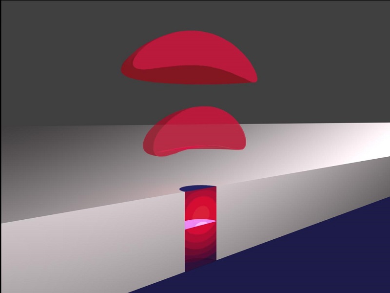
This stylized rendering of the cross-section of the metallic hybrid nanocavity coupled to a quantum dot shows vertical emission into free space. Image credit: Yousif Kelaita, Stanford University
Researchers have developed a new type of light-enhancing optical cavity that is only 200 nanometers tall and 100 nanometers across. Their new nanoscale system represents a step toward brighter single-photon sources, which could help propel quantum-based encryption and a truly secure and future-proofed network.
Quantum encryption techniques, which are seen as likely to be central to future data encryption methods, use individual photons as an extremely secure way to encode data. A limitation of these techniques has been the ability to emit photons at high rates. “One of the most important figures of merit for single-photon sources is brightness — or collected photons per second — because the brighter it is, the more data you can transmit securely with quantum encryption,” said Yousif Kelaita, Nanoscale and Quantum Photonics Lab, Stanford University, California.
In the journal Optical Materials Express, from The Optical Society (OSA), Kelaita and his colleagues show that their new nanocavity significantly increased the emission brightness of quantum dots — nanometer-scale semiconductor particles that can emit single photons.
The researchers created the new nanocavity by using highly reflective silver to coat the sides of a nanoscale semiconductor pillar sitting on a substrate. The silver makes the light bounce around inside the nanopillar, turning it into a very small optical cavity. The researchers say that the same design concept could be used to build nanocavities from other materials that are tailored for different single-photon emitters.
Trapping light in a small space
At nanometer scales, light interacts with materials in unique ways. One example is the Purcell effect, which enhances the emission efficiency of a quantum dot or other light emitter confined in a small cavity. Systems showing Purcell enhancement will emit more photons over a given amount of time, which could enable quantum encryption systems that operate faster than is possible now.
Achieving Purcell enhancement benefits from extremely small cavities because energy is transferred between the light emitter and the cavity more quickly. It is also desirable to have a sufficiently high quality factor, meaning that the cavity’s reflection allows the light to bounce around for a long time.
“We demonstrated a new type of cavity with a volume multiple orders of magnitude lower than the current state of the art in solid-state systems,” said Kelaita. “The system produces strong Purcell enhancement and high light collection efficiency at the same time, which leads to an overall increase in the brightness of the single-photon source.”
When the researchers tested the new nanocavities, they found that the quantum dots placed inside the nanocavities emitted more photons per second than quantum dots not located inside such a cavity.
Because the nanocavities are open on top, emitted light can travel directly into air. Similar nanocavities created previously were topped with a metal coating that was undesirable for collecting emitted photons. The emission profile from the new nanocavities also matches well with standard microscope objective lenses, allowing a high percentage of the light to enter the lens. A mismatch between the emission profile and microscope objective lenses has caused problematic light loss in nanocavity systems developed previously.
Making the tiny cavity
The team used a modified fabrication technique to overcome the challenge of coating the nanopillars with metal. Nanostructures that are tall and skinny tend to experience what are called shadowing effects because nanofabrication techniques use a process in which metal falls straight down onto the device much like snow.
“If you imagine snow falling on a tree, the snow will cling to itself and pile up on a branch in a way that it forms a larger width, or mound, than the branch itself,” said Kelaita. “This also happens as metal is deposited on top of something like a pillar. As the metal clings to itself, it creates a larger mound than the pillar underneath it, preventing metal from falling underneath the parts that eclipse the pillar. In the end, this shadowing effect creates an air gap in the device.”
To solve this problem, the researchers simultaneously rotated and tilted the sample to coat all sides of the pillar at once. Even with this new approach, they had to be careful about the angle at which they deposited the metal to avoid forming a connection between the metal coating the sides of the pillar and the metal on top. If a connection was formed, the final step of ultrasonically removing the metal cap on top would be difficult or impossible.
“Other groups working with metal should be interested in this technique because this shadowing effect occurs even for features that are completely encapsulated in metal,” said Kelaita.
Even better nanocavities
The researchers are now working to create other kinds of nanocavities with even better characteristics. For example, they want to try to make nanocavities in diamond, which could allow single-photon sources that operate at room temperature, a key requirement for incorporating quantum encryption into consumer devices.
They also want to combine the knowledge gained from this new work with an inverse design algorithm they recently developed to automatically design photonic devices integrated onto silicon chips. With the algorithm, engineers specify a desired function and the software provides instructions for making a structure that performs that function.
Filed Under: M2M (machine to machine)


