Design World

  • Home
  • Technologies
    • ELECTRONICS • ELECTRICAL
    • Fastening • joining
    • FLUID POWER
    • LINEAR MOTION
    • MOTION CONTROL
    • SENSORS
    • TEST & MEASUREMENT
    • Factory automation
    • Warehouse automation
    • DIGITAL TRANSFORMATION
  • Learn
    • Tech Toolboxes
    • Learning center
    • eBooks • Tech Tips
    • Podcasts
    • Videos
    • Webinars • general engineering
    • Webinars • Automated warehousing
    • Voices
  • LEAP Awards
  • 2025 Leadership
    • 2024 Winners
    • 2023 Winners
    • 2022 Winners
    • 2021 Winners
  • Design Guides
  • Resources
    • 3D Cad Models
      • PARTsolutions
      • TraceParts
    • Digital Issues
      • Design World
      • EE World
    • Educational Assets
    • Engineering diversity
    • Reports
    • Trends
  • Supplier Listings
  • Advertise
  • SUBSCRIBE
    • MAGAZINE
    • NEWSLETTER

Plant To Produce Larger Solar Panels

By Design World Staff | April 20, 2007

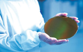
Photovoltaic electric power may light up homes sooner than once believed. Moser Baer India Ltd., selected Applied Materials, Inc., to develop and install the world’s first generation (Gen) 8.5 Thin Film Solar Module Production Line in New Delhi, India. Its expected completion is in the second half of calendar 2007. The line will manufacture photovoltaic solar modules using ultra-large 5.7m2 substrates (2.2 x 2.6 m). These glass panels are four times bigger than today’s largest solar panel substrates.

The contract between Moser Baer and Applied is for a fully-integrated production line including CVD1, PVD2, laser scribing, factory software, automation, and other supporting technologies required to establish a solar panel manufacturing facility with a rated initial capacity of 40 MW per year. “It will be the first truly modern solar facility in India using semiconductor manufacturing processes,” said Mr. Ravi Khanna, CEO, Moser Baer Photo Voltaic Business. The Gen 8.5 Line is flexible; production output can be configured for final product sizes from 1.4 to 5.7 m2. Current thin film production lines are configured for panel sizes less than 1.5 m2.

“We are focused on developing and manufacturing innovative products that significantly reduce electric power and utility costs and provide a cost-effective option for clean renewable energy,” continued Khanna. By 2009, Moser plans to step-up its 40-MW plant to a full 200-MW solar panel facility.

“This contract signals a critical milestone for the solar industry in the drive to reduce the cost of solar cells by using larger substrates,” said Mark Pinto, senior vice president and general manager of Applied’s New Business and New Products Group.

Moser Baer India Ltd.
www.moserbaer.com
Applied Materials, Inc.
www.appliedmaterials.com

:: Design World ::

You might also like


Filed Under: Semiconductor manufacture


LEARNING CENTER

Design World Learning Center
“dw
EXPAND YOUR KNOWLEDGE AND STAY CONNECTED
Get the latest info on technologies, tools and strategies for Design Engineering Professionals.
Motor University

Design World Digital Edition

cover

Browse the most current issue of Design World and back issues in an easy to use high quality format. Clip, share and download with the leading design engineering magazine today.

EDABoard the Forum for Electronics

Top global problem solving EE forum covering Microcontrollers, DSP, Networking, Analog and Digital Design, RF, Power Electronics, PCB Routing and much more

EDABoard: Forum for electronics

Sponsored Content

  • Digitalization made easy: Bridging IT/OT with scalable network infrastructure
  • Apple Rubber custom o-rings for harsh underwater conditions
  • ASMPT chooses Renishaw for high-quality motion control
  • Innovating Together: How Italian Machine Builders Drive Industry Forward Through Collaboration
  • Efficiency Is the New Luxury — and Italy Is Delivering
  • Beyond the Build: How Italy’s Machine Makers Are Powering Smart Manufacturing
View More >>
Engineering Exchange

The Engineering Exchange is a global educational networking community for engineers.

Connect, share, and learn today »

Design World
  • About us
  • Contact
  • Manage your Design World Subscription
  • Subscribe
  • Design World Digital Network
  • Control Engineering
  • Consulting-Specifying Engineer
  • Plant Engineering
  • Engineering White Papers
  • Leap Awards

Copyright © 2025 WTWH Media LLC. All Rights Reserved. The material on this site may not be reproduced, distributed, transmitted, cached or otherwise used, except with the prior written permission of WTWH Media
Privacy Policy | Advertising | About Us

Search Design World

  • Home
  • Technologies
    • ELECTRONICS • ELECTRICAL
    • Fastening • joining
    • FLUID POWER
    • LINEAR MOTION
    • MOTION CONTROL
    • SENSORS
    • TEST & MEASUREMENT
    • Factory automation
    • Warehouse automation
    • DIGITAL TRANSFORMATION
  • Learn
    • Tech Toolboxes
    • Learning center
    • eBooks • Tech Tips
    • Podcasts
    • Videos
    • Webinars • general engineering
    • Webinars • Automated warehousing
    • Voices
  • LEAP Awards
  • 2025 Leadership
    • 2024 Winners
    • 2023 Winners
    • 2022 Winners
    • 2021 Winners
  • Design Guides
  • Resources
    • 3D Cad Models
      • PARTsolutions
      • TraceParts
    • Digital Issues
      • Design World
      • EE World
    • Educational Assets
    • Engineering diversity
    • Reports
    • Trends
  • Supplier Listings
  • Advertise
  • SUBSCRIBE
    • MAGAZINE
    • NEWSLETTER
We use cookies to personalize content and ads, to provide social media features, and to analyze our traffic. We share information about your use of our site with our social media, advertising, and analytics partners who may combine it with other information you’ve provided to them or that they’ve collected from your use of their services. You consent to our cookies if you continue to use this website.