By Geoff Shannon, Laser Technology Manager, and Paul Severloh, Engineer, Miyachi Unitek
Micro welding of conductive materials such as copper is difficult, but a green laser (532 nm) offers a useful non-contact joining method, which also happens to be well geared for automatic applications.
Connecting conductive parts to achieve electrical contact is required in almost every industry. The technologies used to make these connections are driven by cost, joint performance, and volume requirements.
As part miniaturization continues and connector sizes decrease below 0.004-in. thick for flat ribbons and wire diameters, traditional processes such as crimping, soldering, and brazing become less viable due to high joint resistance, questionable joint reliability, and longevity. By contrast, welding, which provides excellent joint integrity, longevity, and conduction performance, is quickly becoming standard. The technology required to join two materials where at least one is less than 0.02-in. in thickness is called “micro welding.”
Copper is typically the material of choice for connecting conductive parts with micro welding because of its ability to efficiently conduct electrical energy and transmit signals. However, the very high thermal conductivity that makes copper such a good choice as a conductor rapidly pulls heat away from the weld joint, making it difficult to maintain heat balance and weld reliably. This difficulty is further exacerbated by increased production rates, reduced part size, and welding of dissimilar materials and dissimilar conductor cross sections.

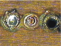
Here is an example of typical spot welds on bare
copper using a 1064 nm (bottom) and 532 nm
pulsed Nd:YAG laser (top).
The challenge of micro welding copper is how to control the heat balance in these small and highly conductive parts to enable welding while ensuring no over- or under-heating. One way to meet this challenge is by using a 532 nm, or green, wavelength.
Pluses and minuses of traditional micro welding techniques
Micro welding can be done using several options: ultrasonic bonding, resistance welding, and laser welding. Each has its advantages and disadvantages and each meets micro-welding requirements somewhat differently.
Ultrasonic bonding uses vibration energy at the joint interface to create the bond. The vibration energy is delivered to the interface by a sonotrode or horn that contacts the top part. The horn vibrates at frequencies of hundreds to thousands of times per second with a motion amplitude between 0.0005 to 0.004-in. The underside of the part is supported with an “anvil,” which can be either static or also vibrating.
This vibratory action under applied force causes plastic deformation of surface disparities at the weld interface, leading to highly intimate contact and a diffusing of metallic atoms. The joint forms by diffusion; there is no melting at the joint. There is some deformation or thickness reduction of the parts, but this can normally be controlled. Contact of the horn to the part is maintained by the horn’s friction, enhanced by a knurling pattern on the horn along with a force applied on the parts.

Ultrasonic welding is particularly well suited to sheet welding of conductive parts, including aluminum and copper. It has some drawbacks for micro welding. Since force is imparted onto the parts, mechanical contact is required on either side of the joint. Also, the horn is a consumable that requires inspection and replacement. Joint geometry is somewhat limited to lap welding only. Finally, the speed of the welding cycle that involves actuation of the horn can slow production rates.
Resistance welding uses the weld interface’s high resistance to create heat as current is passed through the parts. The circuit is created by electrodes that contact the part either from the same side or opposite sides of the work pieces. Electrical contact is assured by exerting some force on the parts.
When resistance welding conductive parts, the electrodes are resistive and therefore perform two functions: they heat up and conduct heat to the parts and they conduct sufficient current to enable some heating to occur at the joint interface.
Resistance welding works well for a variety of joining applications and materials. However, since this process relies on mechanical contact and the need to create an electrical circuit between two electrodes, it may not work properly in all circumstances, especially if the parts are mechanically delicate. In addition, the minimum electrode size is around 0.04-in. in diameter, and so this may limit joint accessibility.
Laser welding is a non-contact process requiring only single-sided access. The technology is useful for working on extremely small joint areas and can be used to weld different shaped parts, different joint geometries, and dissimilar materials. No consumables are used that need to be maintained or replaced and the weld cycle is milliseconds. On the face of it, laser welding appears to be an excellent solution for copper micro welding – but there is a problem. The pulsed Nd:YAG (neodymium-doped yttrium aluminum garnet) used for the majority of micro welding applications has a wavelength of 1064 nm, which is more than 90% reflected by copper.
Initially, extremely high power is needed to overcome the reflectivity and ensure that enough light energy is delivered to the copper. Once laser power reaches the copper and raises its temperature, the reflectivity decreases. But, because laser energy is absorbed in less than a billionth of a second, there is a rapid change in how much more power is absorbed. The high power initially required now far exceeds what is required to form the weld. As a result, the material rapidly overheats and vaporizes, leaving a hole.
A number of techniques have been used to overcome this reflectivity, including pulse shaping, oxygen assist, and the use of less reflective platings. Pulse shaping, however, is not reliable because the reflectivity of copper and other conductive parts varies, and so the precise moment at which the laser power should be reduced also varies. There have been some attempts to better anticipate this “precise moment” by implementing feedback techniques, but none have so far proven viable.
Oxygen has been shown to dramatically increase penetration in seam welding copper by building an oxide layer on the part to be welded, but this has not been effective for spot welding applications because the positive effect of oxygen is seen only after several successive pulses and so does not offer a reliable technique for single spot welding or short seams. Using less reflective coatings such as nickel or tin does help to reduce initial reflection, but does not fully alleviate the problem, as large energies are still required to continue the coupling into the copper; thus the process window for micro welding becomes very small.
Material reflectivity must be addressed to achieve a good, strong laser micro weld on copper. Reducing the wavelength from 1064 nm to 532 nm significantly reduces the reflectivity of copper and other conductive materials. This wavelength enables consistent coupling into the copper and stabilizes welding. At 532 nm, the laser couples into copper as 1064 nm couples into steel. Therefore, successful micro welding of copper can be achieved if a 532 nm laser is used.
You can achieve this wavelength in two ways. Most common is to use a q-switched laser, but such a laser does not have sufficient pulse energy to weld.
A more novel approach is to use a regular pulsed Nd:YAG laser, which offers 532 nm light at 1.5 kW peak power with up to a 5 ms pulse width. This provides enough weld energy to penetrate approximately 350 µm thick copper, which is sufficient for most micro welding applications. Another benefit of a pulsed Nd:YAG laser delivered through a fiber is that the beam has low brightness, which promotes even absorption across the focus spot, preventing hot spots at the center of the weld that may cause instability.
Electrical connections come in different sizes, shapes, and materials. The welding of electrical contacts needs to be a seamless process to the operation of the part, such that the joint performs as a single solid continuous component. Laser welding offers this potential.
For example, the automotive industry has seen a significant increase in sensor technology to monitor car performance, function, and environment. Each sensor has many terminal connections that must survive for the lifetime of the car. In this arena, laser micro welding offers a viable option, and the laser provides a great tool for high speed high quality welding.
Connection requirements are also critical in the medical industry, for example in implantable devices, sensing and monitoring instruments, where each connection is critical to maintaining part function and performance, and thus requires a highly stable joining technology.
Similarly, in the communications industry, signal strength and integrity are crucial to maximize part performance and ensure that the joint is not a limiting factor to the part’s design.
Micro welding of such conductive materials as copper can be difficult, but laser welding offers a useful non-contact joining method. In the past, copper’s reflectivity at the 1064 nm wavelength has always been the barrier to implementing laser welding. The use of a 532 nm green Nd:YAG laser welder removes this barrier, offering a viable method for micro welding copper and other conductive materials in high volume.
Green laser welding across industry
There are a number of electrical contact configurations needed across all industries chosen according to specific part and component design. Here’s a look at a few of the connection options that can be accomplished using the pulsed green laser.
Flat ribbon to thick film metalized pad
A common connection in the electronics industry is where a 0.00150-in. thick gold-coated copper flat wire is bonded to metallized pads. Ideally the pad thickness is at least 1.5 times the thickness of the ribbon, because this creates a good thermal balance between the wire and the pad preventing the pad from overheating.

Wire to metalized pad/terminal
To join solid and stranded wires in power electronics applications, position the laser to the tip of the wire and the pad. The wire will effectively reflow on the pad. The key in welding a stranded wire is maintaining the tip to ensure the strands are closely packed. You can achieve this by compacting, dipping in a plating, or using a short cut back distance to the insulation.
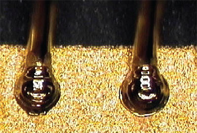
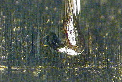
Side by side square terminal to round wire
The flexibility of the laser is extremely valuable in welding different joint geometries and terminal shapes. The weld of a gold-plated copper connector to a silver-plated copper wire, for example, is made in a butt configuration, with the position of the wire in relation to the terminal showing some variation plus the gap between the wire round and the square edge of the terminal. The controlled and consistent absorption of the laser power to both parts enables a reliable weld.


Flat to flat lead frame connections
For high volume production, welding multiple joints on lead frames is all about quality and speed. Being a non-contact process, laser welding lends itself to volume manufacturing. It can execute many welds per second, according to the motion integration.
Miniature lithium ion/polymer battery connections
Power application that require less than 50 mAh for such applications as wireless products, smart cards, or RFID tags, generally use either lithium ion or lithium polymer battery technology. For these applications that require the battery terminal to be connected, there are a number of special challenges. Each terminal is made of copper and aluminum, which are both problematic to weld. The terminal material is also thin, sometimes less than 0.001-in. In some applications, ultrasonic welding is used, but laser welding is also an option, and may be especially well suited to joining terminals to PCB metalized pads.

Micro welding of dissimilar materials
When welding materials with different levels of absorption, there is a tendency to overheat the more absorptive materials, causing excessive spatter and porosity. This situation is usually overcome by favoring one material. However, for small parts, this may not be sufficient because even the tiniest absorption imbalance can create an overheated weld. At 532 nm wavelength, the reflection of both parts becomes closer, therefore the weld energy balances more consistently, significantly improving the weld.

Miyachi Unitek
www.miyachiunitek.com/
::Design World::
Filed Under: Automotive, Green engineering • renewable energy • sustainability, FASTENING • JOINING • locks • latches • pins






Tell Us What You Think!