As a hard and brittle material, silicon has practically no natural elasticity. But in a new study, researchers have demonstrated that amorphous silicon can be grown into superelastic horseshoe-shaped nanowires that can undergo stretching of more than twice their original length, and still maintain their excellent electric properties.
The results are exciting news for the area of stretchable electronics, as they suggest that silicon nanowire springs could serve as a stretchable semiconducting material for future flexible, bendable electronic devices. So far, almost all of the stretchable electronics that have been demonstrated have been made of polymer and organic semiconductors, whose semiconducting properties are inferior to those of silicon.
The researchers, who are from Nanjing University, Peking University, and CNRS-Ecole Polytechnique, have published a paper on their new method for growing stretchable silicon springs in a recent issue of Nano Letters.
In previous efforts to fabricate stretchable silicon, some of the best results have come from using electron beam lithography. In this technique, ultra-thin crystalline silicon is etched into various patterns, such as serpentine shapes and fractal patterns, that endow the resulting silicon device with stretchability. However, electron beam lithography is expensive and impractical for fabricating large-area electronics.
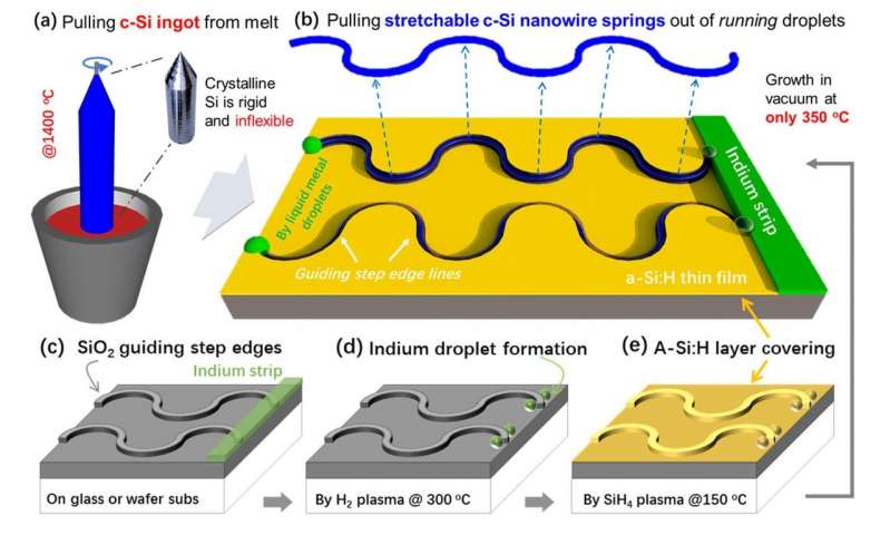
As the researchers explain in the new paper, one ideal and relatively inexpensive method for making stretchable silicon nanowires would be similar to the crystal pulling methods used to grow silicon crystal ingots from molten silicon. In these methods, which are widely used in the silicon industry, a seed crystal is dipped in molten silicon and slowly pulled upward, drawing with it a long crystalline silicon ingot.
As the researchers explain, the new method is somewhat like a nanoscale, in-plane version of crystal pulling. The process, called line-shape engineering, involves guiding molten indium droplets to move along a pre-patterned track that is coated with amorphous silicon. As the droplet moves along the track, it takes in amorphous silicon and precipitates crystalline silicon nanowires.
In their demonstrations, the researchers grew crystalline silicon nanowires more than a millimeter long into patterns such as horseshoe shapes and a Peano curve, which has previously been shown to be one of the best fractal patterns for achieving large stretchability. In previous work, the researchers had demonstrated the guided growth of silicon nanowires in straight lines, but the ability to grow them in tightly curved patterns like these is essential for achieving stretchability. Tests revealed that the springs can be pulled to more than twice their original length—almost into a straight line—while maintaining their electric properties and quickly recovering their original shape when released.
In the future, the researchers plan to investigate techniques for transferring the silicon nanosprings from the growth substrate onto a softer surface that is more practical for applications. Overall, they expect that the growth method demonstrated here represents an important step toward developing high-performance, stretchable silicon electronics.
“In view of future industrial applications, the fabrication can be extremely low-cost and scalable, so that the size of a 1D spring array can be several meters wide and rollable in production,” coauthor Linwei Yu, at Nanjing University and Peking University, told Phys.org. “Our vision is to define a new wafer technology, catering to the needs of large-area electronics, that offers batch-manufacturable, robust, and stretchable crystalline silicon channels to instill good performance into the emerging soft electronics. Our latest progress has demonstrated a complete free-standing network of such silicon springs. An immediate application will be deploying them upon skin for sensors, as well as mechanical devices, field-effect devices, and NEMS. Hopefully, these new results will come out soon.”
Filed Under: Materials • advanced