Design World

  • Home
  • Technologies
    • 3D CAD
    • Electronics • electrical
    • Fastening & Joining
    • Factory automation
    • Linear Motion
    • Motion Control
    • Test & Measurement
    • Sensors
    • Fluid power
  • Learn
    • Ebooks / Tech Tips
    • Engineering Week
    • Future of Design Engineering
    • MC² Motion Control Classrooms
    • Podcasts
    • Videos
    • Webinars
  • LEAP AWARDS
  • Leadership
    • 2022 Voting
    • 2021 Winners
  • Design Guide Library
  • Resources
    • 3D Cad Models
      • PARTsolutions
      • TraceParts
    • Digital Issues
      • Design World
      • EE World
    • Women in Engineering
  • Supplier Listings

New Method For Etching Enables Lithium Niobate Chips

By Megan Crouse | January 18, 2018

Share

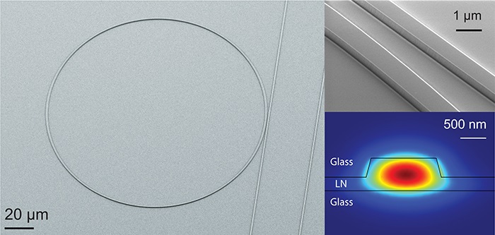
A micro-ring and micro-racetrack resonators made on lithium niobate film. Image credit: Loncar Lab/Harvard SEAS

Researchers at Harvard University have developed a new technique to etch lithium niobate sheets for use in optoelectronics.

Lithium niobate is particularly suited for electro-optics, acousto-optics, and non-linear optics because of its large electro-optic coefficients, but it can be difficult to etch. Chemical etching will not work, so other methods have been tried, many of them time-consuming. The Harvard team has applied plasma reactive ion etching to lithium niobate and found it effective in creating waveguides as well as in minimizing optical power losses.

The first step in the plasma reactive ion etching was to draw patterns for waveguides on a photoresist layer with electron-beam lithography, the same as used in standard silicon etching. This then created a mask that could be placed over niobate film. Argon ions were scattered across the sample (this is the actual plasma reactive ion etching), stripping material away where it had been etched and forming waveguides in that fashion.

“The next step is the integration of the niobate into silicon photonic processing, and that may be challenging because niobium is not a material people in the silicon industry like very much. Maybe we will have to turn to dedicated fabrication facilities that will allow this hybrid electronic integration,” said Marko Lončar, professor of electrical engineering at Harvard’s John A. Paulson School of Engineering and Applied Sciences. “For now, we have to make the niobium chips and the silicon chips separately and couple them together.”

Even without that streamlined process, this technique of creating waveguides produces optical power losses of only 50 percent over 1 meter, the university said.

There is some precedent for manufacturing these at a commercial level: the thin film substrates combined for the plasma reactive ion etching were produced commercially.  


Filed Under: Materials • advanced


Related Articles Read More >

Self-lubricating and wear-resistant: igus bar stock for food, continuous operation and high media resistance
Minnesota Rubber and Plastics announces plans for new Innovation Center
The importance of resin selection
EXE014 - Image 1
Composite materials help place Italian race team in pole position

DESIGN GUIDE LIBRARY

“motion

Enews Sign Up

Motion Control Classroom

Design World Digital Edition

cover

Browse the most current issue of Design World and back issues in an easy to use high quality format. Clip, share and download with the leading design engineering magazine today.

EDABoard the Forum for Electronics

Top global problem solving EE forum covering Microcontrollers, DSP, Networking, Analog and Digital Design, RF, Power Electronics, PCB Routing and much more

EDABoard: Forum for electronics

Sponsored Content

  • Global supply needs drive increased manufacturing footprint development
  • How to Increase Rotational Capacity for a Retaining Ring
  • Cordis high resolution electronic proportional pressure controls
  • WAGO’s custom designed interface wiring system making industrial applications easier
  • 10 Reasons to Specify Valve Manifolds
  • Case study: How a 3D-printed tool saved thousands of hours and dollars

Design World Podcasts

May 17, 2022
Another view on additive and the aerospace industry
See More >
Engineering Exchange

The Engineering Exchange is a global educational networking community for engineers.

Connect, share, and learn today »

Design World
  • Advertising
  • About us
  • Contact
  • Manage your Design World Subscription
  • Subscribe
  • Design World Digital Network
  • Engineering White Papers
  • LEAP AWARDS

Copyright © 2022 WTWH Media LLC. All Rights Reserved. The material on this site may not be reproduced, distributed, transmitted, cached or otherwise used, except with the prior written permission of WTWH Media
Privacy Policy | Advertising | About Us

Search Design World

  • Home
  • Technologies
    • 3D CAD
    • Electronics • electrical
    • Fastening & Joining
    • Factory automation
    • Linear Motion
    • Motion Control
    • Test & Measurement
    • Sensors
    • Fluid power
  • Learn
    • Ebooks / Tech Tips
    • Engineering Week
    • Future of Design Engineering
    • MC² Motion Control Classrooms
    • Podcasts
    • Videos
    • Webinars
  • LEAP AWARDS
  • Leadership
    • 2022 Voting
    • 2021 Winners
  • Design Guide Library
  • Resources
    • 3D Cad Models
      • PARTsolutions
      • TraceParts
    • Digital Issues
      • Design World
      • EE World
    • Women in Engineering
  • Supplier Listings