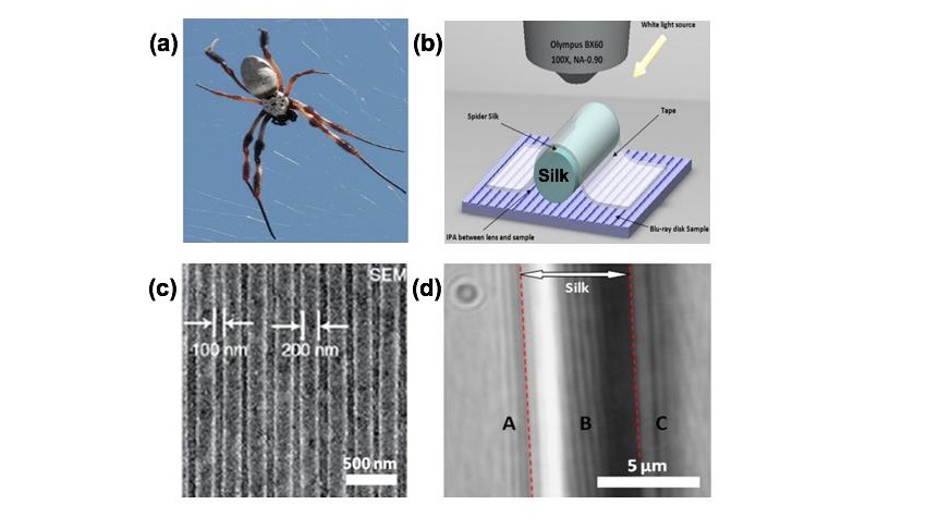
(a) Nephila edulis spider in its web. (b) Schematic drawing of reflection mode silk biosuperlens imaging. The spider silk was placed directly on top of the sample surface by using a soft tape, which magnify underlying nano objects 2-3 times (c) SEM image of Blu-ray disk with 200/100 nm groove and lines (d) Clear magnified image (2.1x) of Blu-ray disk under spider silk superlens. Image credit: Bangor University/ University of Oxford
Scientists at the UK’s Bangor and Oxford universities have achieved a world first: using spider-silk as a superlens to increase the microscope’s potential.
Extending the limit of classical microscope’s resolution has been the ‘El Dorado’ or ‘Holy Grail’ of microscopy for over a century. Physical laws of light make it impossible to view objects smaller than 200 nm – the smallest size of bacteria, using a normal microscope alone. However, superlenses which enable us to see beyond the current magnification have been the goal since the turn of the millennium.
Hot on the heels of a paper (Sci. Adv. 2 e1600901,2016) revealing that a team at Bangor University’s School of Electronic Engineering has used a nanobead-derived superlens to break the perceived resolution barrier, the same team has achieved another world first.
Now the team, led by Dr Zengbo Wang and in colloboration with Prof. Fritz Vollrath’s silk group at Oxford University’s Department of Zoology, has used a naturally occurring material – dragline silk of the golden web spider, as an additional superlens, applied to the surface of the material to be viewed, to provide an additional 2-3 times magnification.
This is the first time that a naturally occurring biological material has been used as a superlens.
In the paper in Nano Letters (DOI: 10.1021/acs.nanolett.6b02641, Aug 17 2016), the joint team reveals how they used a cylindrical piece of spider silk from the thumb sized Nephila spider as a lens.
“We have proved that the resolution barrier of microscope can be broken using a superlens, but production of manufactured superlenses invovles some complex engineering processes which are not widely accessible to other reserchers,” said Wang. “This is why we have been interested in looking for a naturally occurring superlens provided by ‘Mother Nature’, which may exist around us, so that everyone can access superlenses.”
“It is very exciting to find yet another cutting edge and totally novel use for a spider silk, which we have been studying for over two decades in my laboratory,” said Vollrath.
These lenses could be used for seeing and viewing previously ‘invisible’ structures, including engineered nano-structures and biological micro-structures as well as, potentially, native germs and viruses.
The natural cylindrical structure at a micron- and submicron-scale make silks ideal candidates, in this case, the individual filaments had diameters of one tenth of a thin human hair.
The spider filament enabled the group to view details on a micro-chip and a blue- ray disk which would be invisible using the unmodified optical microscope.
In much the same was as when you look through a cylindrical glass or bottle, the clearest image only runs along the narrow strip directly opposite your line of vision, or resting on the surface being viewed, the single filament provides a one dimensional viewing image along its length.
“The cylindrical silk lens has advantages in the larger field-of-view when compared to a microsphere superlens. Importantly for potential commercial applications, a spider silk nanoscope would be robust and economical, which in turn could provide excellent manufacturing platforms for a wide range of applications,” Wang said.
Filed Under: Rapid prototyping