Design World

  • Home
  • Technologies
    • 3D CAD
    • Electronics • electrical
    • Fastening & Joining
    • Factory automation
    • Linear Motion
    • Motion Control
    • Test & Measurement
    • Sensors
    • Fluid power
  • Learn
    • Ebooks / Tech Tips
    • Engineering Week
    • Future of Design Engineering
    • MC² Motion Control Classrooms
    • Podcasts
    • Videos
    • Webinars
  • LEAP AWARDS
  • Leadership
    • 2022 Voting
    • 2021 Winners
  • Design Guide Library
  • Resources
    • 3D Cad Models
      • PARTsolutions
      • TraceParts
    • Digital Issues
      • Design World
      • EE World
    • Women in Engineering
  • Supplier Listings

Ultraflat Magnets: Atom-Thick Alloys With Unanticipated Magnetic Properties

By Rice University | October 13, 2017

Share

Substituting atoms in the process of making two-dimensional alloys not only allows them to be customized for applications but also can make them magnetic, according to Rice University scientists and their collaborators.

A new paper in Advanced Materials outlines how researchers at Rice, Oak Ridge National Laboratory, the University of Southern California (USC) and Kumamoto University in Japan used chemical vapor deposition (CVD) to make atom-thick sheets and, in the same step, tailor their properties by adding other elements through a process known as doping.

They discovered by surprise that they could also give the 2-D sheets magnetic properties.

The labs worked with transition metal dichalcogenides, alloys that combine a transition metal and chalcogen atoms into a single material. Transition metals are stable elements that fall in the middle of the periodic table. Chalcogens include sulfur, selenium and tellurium, also neighbors to each other in the table.

By adding a dopant element to the mix during CVD, the researchers showed it was possible to rearrange the atoms on the resulting 2-D crystal sheets. They demonstrated several different configurations and found they could replace some atoms outright with the dopant. These physical changes led to changes in the mechanical and electronic properties of the flat crystals, said co-author and Rice postdoctoral researcher Chandra Sekhar Tiwary.

The Rice lab of Pulickel Ajayan led the project to test theories by USC researchers who calculated that doping the materials would force a phase transition in the 2-D crystals. The Rice team confirmed the theory that adding rhenium in various amounts to molybdenum diselenide during growth would allow them to tailor its properties by changing its atomic structure. The magnetic signatures were a bonus.

“Usually, when you make a magnetic material, you start with magnetic elements like iron or cobalt,” said graduate student and co-lead author Amey Apte. “Rhenium, in bulk, is not a magnetic material, but it turns out it is in certain combinations at the atomic scale. It worked fantastically in this case.”

The researchers said the magnetic properties they discovered could make the 2-D alloys of interest to those who design spintronic devices.

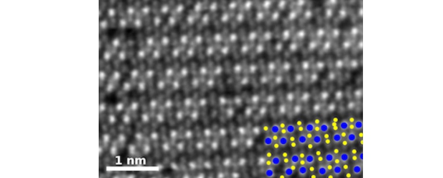
A high-angle annular dark-field image of pure rhenium diselenide. In the key at bottom right, rhenium atoms are blue and selenium atoms yellow. Image credit: Image by Oak Ridge National Laboratory


Filed Under: Materials • advanced


Related Articles Read More >

Self-lubricating and wear-resistant: igus bar stock for food, continuous operation and high media resistance
Minnesota Rubber and Plastics announces plans for new Innovation Center
The importance of resin selection
EXE014 - Image 1
Composite materials help place Italian race team in pole position

DESIGN GUIDE LIBRARY

“motion

Enews Sign Up

Motion Control Classroom

Design World Digital Edition

cover

Browse the most current issue of Design World and back issues in an easy to use high quality format. Clip, share and download with the leading design engineering magazine today.

EDABoard the Forum for Electronics

Top global problem solving EE forum covering Microcontrollers, DSP, Networking, Analog and Digital Design, RF, Power Electronics, PCB Routing and much more

EDABoard: Forum for electronics

Sponsored Content

  • Pushing performance: Adding functionality to terminal blocks
  • Get to Know Würth Industrial Division
  • Renishaw next-generation FORTiS™ enclosed linear encoders offer enhanced metrology and reliability for machine tools
  • WAGO’s smartDESIGNER Online Provides Seamless Progression for Projects
  • Epoxy Certified for UL 1203 Standard
  • The Importance of Industrial Cable Resistance to Chemicals and Oils

Design World Podcasts

June 12, 2022
How to avoid over engineering a part
See More >
Engineering Exchange

The Engineering Exchange is a global educational networking community for engineers.

Connect, share, and learn today »

Design World
  • Advertising
  • About us
  • Contact
  • Manage your Design World Subscription
  • Subscribe
  • Design World Digital Network
  • Engineering White Papers
  • LEAP AWARDS

Copyright © 2022 WTWH Media LLC. All Rights Reserved. The material on this site may not be reproduced, distributed, transmitted, cached or otherwise used, except with the prior written permission of WTWH Media
Privacy Policy | Advertising | About Us

Search Design World

  • Home
  • Technologies
    • 3D CAD
    • Electronics • electrical
    • Fastening & Joining
    • Factory automation
    • Linear Motion
    • Motion Control
    • Test & Measurement
    • Sensors
    • Fluid power
  • Learn
    • Ebooks / Tech Tips
    • Engineering Week
    • Future of Design Engineering
    • MC² Motion Control Classrooms
    • Podcasts
    • Videos
    • Webinars
  • LEAP AWARDS
  • Leadership
    • 2022 Voting
    • 2021 Winners
  • Design Guide Library
  • Resources
    • 3D Cad Models
      • PARTsolutions
      • TraceParts
    • Digital Issues
      • Design World
      • EE World
    • Women in Engineering
  • Supplier Listings