The rapid proliferation of vision technology in embedded systems has led to ultra-high-speed imaging solutions for automotive safety, machine vision, and motion analysis. That, in turn, translates into a significant boost in performance and imaging capabilities via more powerful image sensors and smaller pixel architectures.
Machine vision technology uses image-recognition algorithms to identify the object within the image and facilitate a more detailed and accurate picture of the object without distortion in a broad array of applications, such as industrial automation, robotics, agricultural drones, and 3D modeling.
For a start, the small but powerful processor platforms are driving down traditional machine vision system costs. Next, a new breed of image sensors, aided by powerful, low-cost, and energy-efficient processing, is quickly evolving to address the needs of industrial-grade imaging applications like optical inspection and industrial automation.
The image sensor, a key ingredient in any machine vision design, is going through a rapid makeover on both speed and resolution frontiers. New image sensors are achieving higher frame rates without any compromise in image quality. And, for resolution, these image sensors feature robust optical format to ensure imaging detail and performance needed for modern machine vision and inspection use cases.
Moreover, these low-power embedded systems can support multiple product resolutions while catering to a wide range of pixel functionality. In these embedded vision systems, which are quickly evolving with new pixel architectures, larger pixels can trade resolution at a given optical format for higher imaging sensitivity.
Beyond the Factory Floor
Machine vision, as market research firm Yole Développement puts it, is at the heart of industrial automation revolution. However, it’s important to note that machine vision is much more than merely giving eyes to industrial robots. It encompasses almost all machines and all aspects of the manufacturing cycle.
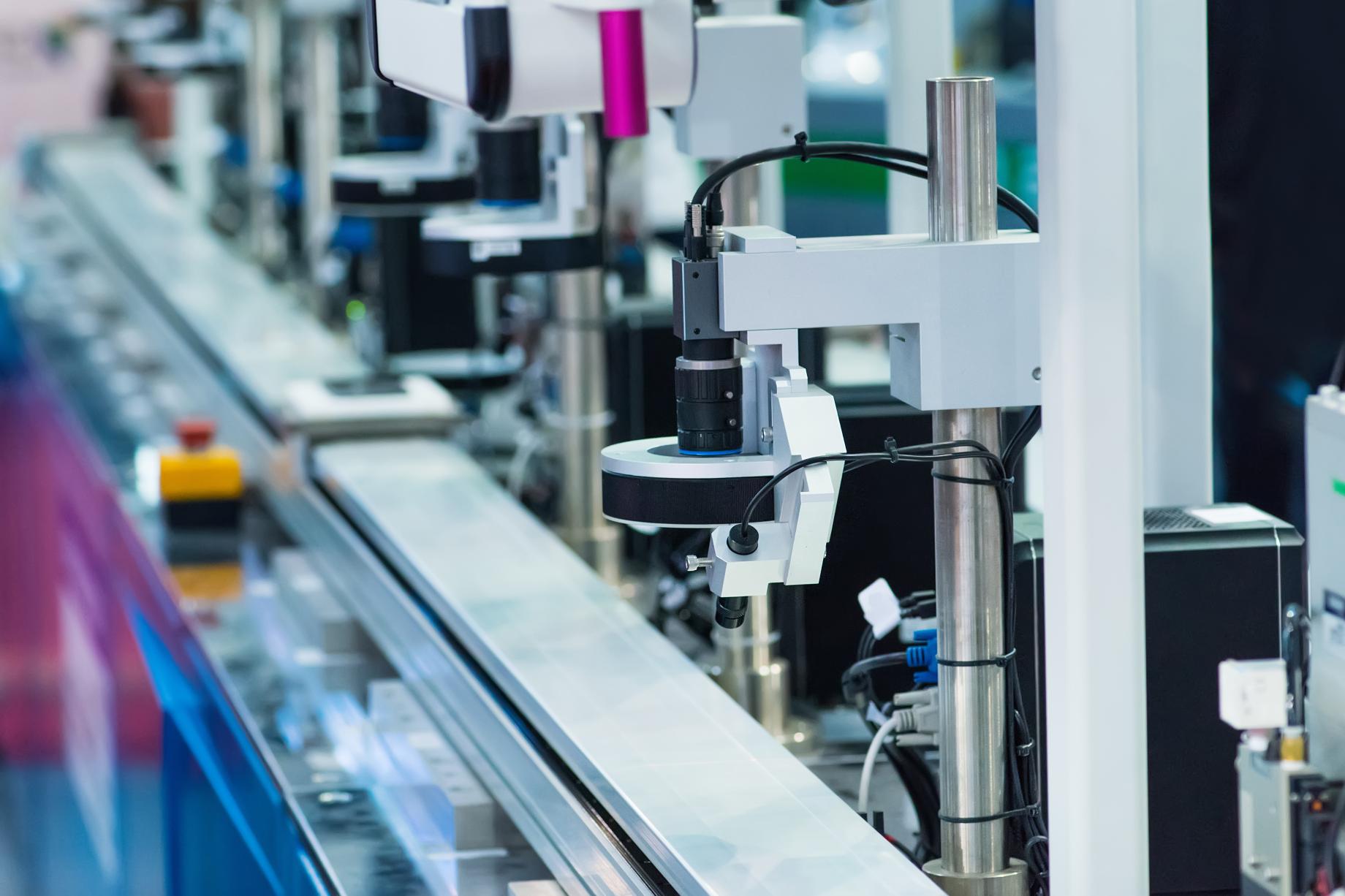
Figure 1: Machine vision technology is taking factory automation beyond its current capabilities. (Image Source: ams AG)
In fact, machine vision is serving a lot of applications outside the factory floor. The use of machine vision spans from vehicle number plate recognition in intelligent traffic systems to tracking movements of customers and items in cashier-less stores to becoming the eyes of self-driving vehicles.
It’s no secret now that machine learning has become a key enabling technology in the autonomous-car movement. Even now, it’s playing a vital role in advanced driver-assistance systems (ADAS), where multiple machine vision algorithms deliver impeccable perception accuracy.
Machine vision is also performing intelligent video content analytics for several camera-centric use cases that include surveillance, as well as augmented reality (AR) and virtual reality (VR) headsets and accessories. Take the example of global shutter image sensors from OmniVision Technologies targeted at applications like agricultural drones.
The 2-megapixel image sensors feature a 15-degree chief ray angle (CRA) to support wide field-of-view lens, and thus, efficiently capture high-resolution images for crop and field monitoring.
OmniVision’s OG02B10 provides color images while the more cost-effective OG02B1B sensor offers the monochrome image, and both devices are available in a 1/2.9-in. optical format. These image sensors employ global shutter sensor technology to eliminate motion artifacts and blurring effects.
That brings us to a major technology shift in machine vision sensor designs: global shutter scanning.
Why Global Shutter
Global shutter, creating a new dimension in camera design, enables superior imaging performance, high image uniformity, and low noise. Unlike rolling shutter, global shutter technology enables the sensor to scan the entire area of an image simultaneously, a critical requirement in machine vision applications.
Another global shutter image sensor targeted at machine vision applications is CSG14k from Premstaetten, Austria-based sensor supplier ams AG. It features correlated double sampling (CDS) technology to create high-quality images of fast-moving objects in robotics, sorting equipment, laser triangulation, and measurement instrumentation.
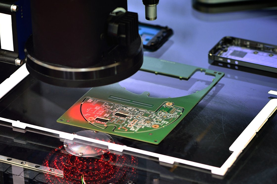
Figure 2: The CSG14k image sensor features a 3840 x 3584 pixel array and 14 megapixel resolution for robotics and other factory automation applications. (Image Source: ams AG)
The 12-bit image sensor claims to have a pixel design that is 66 percent smaller than the previous generation of 10-bit image sensors from ams. That leads to significantly lower noise and high-quality images free of motion artifacts. Then, there are various configuration options in the image sensor that can be tuned for specific application requirements.
The configuration settings help embedded developers optimize designs for low-noise operation. They can also be used to increase dynamic range in order to extract maximum image detail in high-contrast scenes. Additionally, developers can implement low-power modes at a reduced frame rate.
From CCD to CMOS
Another major shift in the machine vision realm relates to the move from charge-coupled device (CCD) image sensors to more economical CMOS-based camera systems that also consume less power and offer higher frame rates. This remarkable technology shift—which kickstarted in consumer imaging in the 1990s and photography sensors in the early 2000s—is now turning machine vision designs upside down.
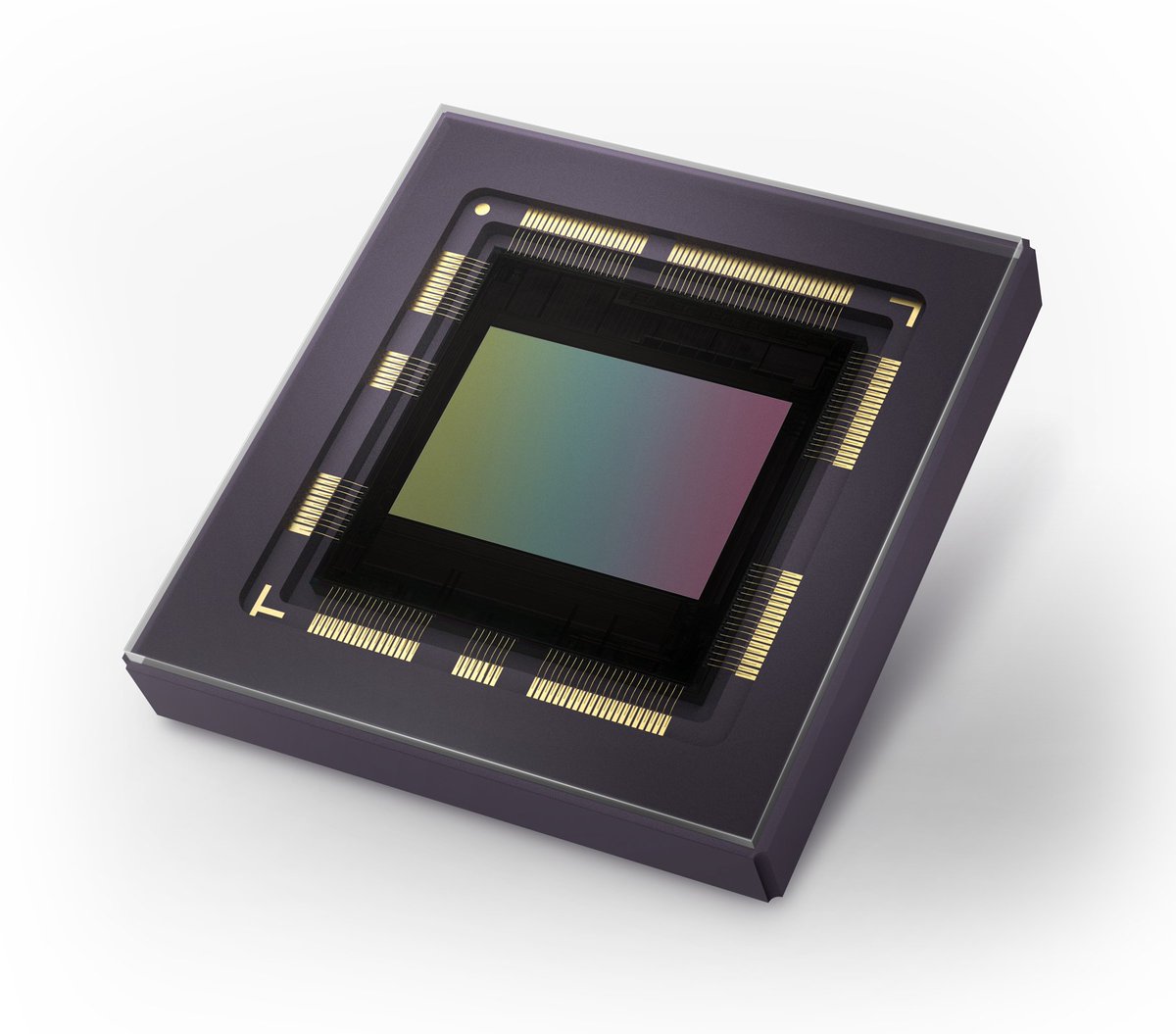
Figure 3: The Emerald 5M is a CMOS image sensor designed for machine vision applications like automated optical inspection (AOI). (Image Source: Teledyne e2v)
The CMOS image sensors have been making strides on two major fronts: image rate and noise level. For embedded vision systems, CMOS sensors are increasingly becoming a technology of choice due to improved noise characteristics. And, CMOS image sensors provide a more detailed view of larger surface areas, a vital demand in factory-automation environments.
The CMV50000 image sensor from ams is a case in point. The global shutter targeting machine learning applications, like automated optical inspection, has replaced the CCD image sensor with a CMOS device that is cheaper and easier to implement.
The 48 megapixel CMOS image sensor features low-noise pixel architecture to produce distortion-free images of fast-moving objects on production lines. It also features on-chip noise-reduction circuitry—black-level clamping—to capture high-quality images even in low-light conditions.
The CMV50000 image sensor, available in a 35-mm format, is based on an eight-transistor pixel architecture. It operates at a fast capture rate of 30 frames/s with 12-bit pixel depth at full resolution or at binned 4K and 8K modes. Also, using the pixel sub-sampling mechanism at 4K resolution, the CMOS image sensor can increase the frame rate to 60 frames/s.
Vision Transformation Underway
Machine vision, a key manifestation of artificial intelligence (AI) revolution, has moved from academic research to the commercial arena. The machine vision systems, for instance, are now widely used in automated optical inspection for testing displays of mobile phones, tablets, laptops, and TVs.
A more specific example is Swatch, which claims that the manufacturing of its mechanical watch Sistem51 is now fully automated. Likewise, contract manufacturer Foxconn, which also produces iPhones, has deployed a million robots for manufacturing consumer electronic goods.
The design case studies outlined in this article demonstrate how next-generation camera designs are filling a void that currently exists between traditional machine vision and consumer electronic imaging systems. And here the shift from CCD to CMOS image sensors has been a key enabler.
The CMOS-centric camera designs are helping developers address extreme processing requirements and low-power constraints in machine vision applications. In short, a major transformation is underway for the creation of lean camera designs to serve motion analysis, robotics, tracking, industrial inspection, and metrology.
Filed Under: AI • machine learning, Industrial automation, Virtual reality