Design World

  • Home
  • Technologies
    • 3D CAD
    • Electronics • electrical
    • Fastening & Joining
    • Factory automation
    • Linear Motion
    • Motion Control
    • Test & Measurement
    • Sensors
    • Fluid power
  • Learn
    • Ebooks / Tech Tips
    • Engineering Week
    • Future of Design Engineering
    • MC² Motion Control Classrooms
    • Podcasts
    • Videos
    • Webinars
  • LEAP AWARDS
  • Leadership
    • 2022 Voting
    • 2021 Winners
  • Design Guide Library
  • Resources
    • 3D Cad Models
      • PARTsolutions
      • TraceParts
    • Digital Issues
      • Design World
      • EE World
    • Women in Engineering
  • Supplier Listings

Solar module manufacturing line standardizes production

By Design World Staff | October 9, 2007

Share

Scientists have long been hopeful that solar energy will power the future. But its potential has remained largely untapped. One of the key steps to putting solar energy into use on a large scale is to reduce the cost of solar panel production.

Solar or photovoltaic panels are made up of treated silicon cells arranged in series’ of strings that produce electric power when exposed to light. Common types of solar panels include monocrystalline, polycrystalline, and amorphous or thin film. The thin film type is currently the cheapest on the market to produce, and Applied Materials, Inc., has something to do with it.
Applied created a line that lets manufacturers rapidly establish solar panel manufacturing capacity and decrease the cost-per-watt of production.
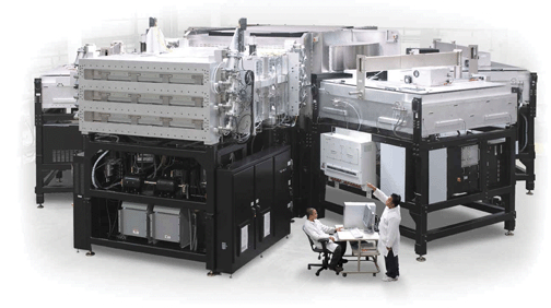
090307.PHOTO.PECVD-1.gif
The Applied SunFab™ Thin Film Line is an integrated production line for manufacturing thin film silicon solar modules using 5.7-meter (m2) glass panels. The 2.2 x 2.6 m substrates are four times bigger than today’s largest thin film solar production panels.


The line can be configured with single or tandem junction technology. It produces enough solar modules per year to generate up to 75 mw of electrical power. The panels can reduce the cost of utility-scale and building-integrated photovoltaic (BIPV) system installations by more than 20 %. The company has already received multiple contracts for its SunFab™ Thin Film Line from customers in Europe and Asia.

Applied adapted its Chemical Vapor Deposition (CVD) and Physical Vapor Deposition (PVD) process systems to build the most critical layers of the module, including its Plasma Enhanced CVD (PECVD) system that processes 5.7m2 glass substrates for the flat panel display industry.

Applied Materials, Inc.
www.appliedmaterials.com

Opera Software ASA
www.opera.com

: Design World :


Filed Under: Semiconductor, Power supplies


Tell Us What You Think!

Related Articles Read More >

Wago-pro2-power-supplies
WAGO Pro2 Power Supplies and DC-to-DC converters from AutomationDirect
Traco Power launches new AC/DC power supplies
ECO 2 power supplies balance size, efficiency with tool-free installation
AutomationDirect-Power-Supply
RHINO power supplies with integrated UPS and Power Boost Technology

DESIGN GUIDE LIBRARY

“motion

Enews Sign Up

Motion Control Classroom

Design World Digital Edition

cover

Browse the most current issue of Design World and back issues in an easy to use high quality format. Clip, share and download with the leading design engineering magazine today.

EDABoard the Forum for Electronics

Top global problem solving EE forum covering Microcontrollers, DSP, Networking, Analog and Digital Design, RF, Power Electronics, PCB Routing and much more

EDABoard: Forum for electronics

Sponsored Content

  • Renishaw next-generation FORTiS™ enclosed linear encoders offer enhanced metrology and reliability for machine tools
  • WAGO’s smartDESIGNER Online Provides Seamless Progression for Projects
  • Epoxy Certified for UL 1203 Standard
  • The Importance of Industrial Cable Resistance to Chemicals and Oils
  • Optimize, streamline and increase production capacity with pallet-handling conveyor systems
  • Global supply needs drive increased manufacturing footprint development

Design World Podcasts

June 12, 2022
How to avoid over engineering a part
See More >
Engineering Exchange

The Engineering Exchange is a global educational networking community for engineers.

Connect, share, and learn today »

Design World
  • Advertising
  • About us
  • Contact
  • Manage your Design World Subscription
  • Subscribe
  • Design World Digital Network
  • Engineering White Papers
  • LEAP AWARDS

Copyright © 2022 WTWH Media LLC. All Rights Reserved. The material on this site may not be reproduced, distributed, transmitted, cached or otherwise used, except with the prior written permission of WTWH Media
Privacy Policy | Advertising | About Us

Search Design World

  • Home
  • Technologies
    • 3D CAD
    • Electronics • electrical
    • Fastening & Joining
    • Factory automation
    • Linear Motion
    • Motion Control
    • Test & Measurement
    • Sensors
    • Fluid power
  • Learn
    • Ebooks / Tech Tips
    • Engineering Week
    • Future of Design Engineering
    • MC² Motion Control Classrooms
    • Podcasts
    • Videos
    • Webinars
  • LEAP AWARDS
  • Leadership
    • 2022 Voting
    • 2021 Winners
  • Design Guide Library
  • Resources
    • 3D Cad Models
      • PARTsolutions
      • TraceParts
    • Digital Issues
      • Design World
      • EE World
    • Women in Engineering
  • Supplier Listings