By Christopher J. Loberg , Tektronix Inc.
Here are tips on ensuring digital signals have good integrity, clean and fast transitions, stable and valid logic levels, accurate placement in time, and are free of any transients.
Evolving technology makes it increasingly difficult for system developers to produce and maintain complete, unimpaired signals in digital systems. Since the beginning of digital technology and the information age (over twenty years since the personal computer emerged and almost as long since cellular telephony went from being a novelty to a consumer necessity), one trend has remained constant: the demand for more features and services; and, the need for more bandwidth to deliver them. First-generation PC users were excited about the power of creating a simple spreadsheet. Now, they demand detailed graphics, high-quality audio, and fast-streaming video.
Along with the information age, a steady stream of technology breakthroughs in the fields of semiconductors has dramatically increased rates, computer applications such as 3D games, and computer-aided design programs. Sophisticated 3D imagery requires a huge amount of bandwidth at the circuit board level. The CPU, graphics subsystem, and the memory must move data constantly as the image moves.
Computers are just one facet of the bandwidth-hungry information age. Digital communication equipment designers (particularly those developing the electrical and optical infrastructure elements for both mobile and fixed networks) are moving toward 40 Gb/s data rates. Digital video product development teams are designing a new generation of transmission equipment for high-definition, interactive video.
Numerous technologies are pushing for higher data rates. Serial buses are emerging to break the speed barriers inherent in older, parallel bus architectures. In some cases, system clocks are intentionally dithered to reduce unintended radiated emissions. Smaller, denser, circuit boards using ball grid array ICs and buried vias have become common as developers look for ways to maximize density and minimize path lengths.
Rising bandwidth challenges
Today’s digital bandwidth race requires innovative thinking. To achieve this improvement, edge speeds today are now a hundred times faster than before. Bus cycle times are up to a thousand times faster than they were twenty years ago. Transactions that once took microseconds are now measured in nanoseconds. Circuit board technology however, has not kept pace because of certain physical realities. The propagation time of inter-chip buses has remained virtually unchanged. Although geometries have shrunk, circuit boards still need sufficient space for IC devices, connectors, passive components, and the bus traces. This space equates to distance, and distance means delay—the enemy of speed.
Signal integrity concepts
At frequencies in the gigahertz range, a host of variables can affect signal integrity: signal path design; impedances and loading; transmission line effects; and power distribution on or off the circuit board. With this in mind, the design engineer’s mission is to minimize these problems from the start and to correct them, when apparent, by investigating both of the fundamental sources of signal degradation: digital and analog issues.
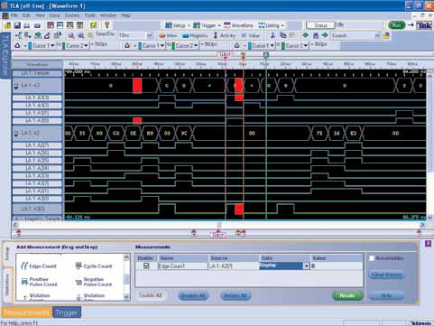
A logic analyzer’s timing resolution determines its ability to detect and display signal deviations.
Digital timing issues
An engineer working with an evolving digital system design is likely to encounter signal integrity problems in its digital form. When binary signals on the bus or device outputs produce incorrect values, the errors may appear in the waveform (timing measurement) view on a logic analyzer, and it may also show up at the state or even the protocol level. It only takes one bad bit to dramatically affect the outcome of an instruction or transaction. Digital signal aberrations stem from many root causes. Timing related issues are especially common:
• Bus contention occurs when two driver devices try to use the same bus line at the same time. Normally, one of the drivers should go to a high impedance state and not hinder the other while it sends data. If the high impedance device doesn’t change in time, the two drivers then contend for the bus. As a result, neither driver prevails. In turn, it forces the bus to an indeterminate amplitude that may fail to reach the threshold voltage. This may create, a “0” logic level where it should be a “1.” With a high-speed bus, this situation is complicated further by the time of flight between the contending sources and the receiver.
• Setup and hold violations increase digital systems push to faster speeds. Known as “setup” time, a clocked device, such as a D flip flop, requires the data to be stable at its input for a specified time before the clock arrives. Similarly, for “hold” time, the input data must remain valid for a specified time after the leading edge of the clock. Violating setup and hold requirements can cause unpredictable glitches on the output, or cause no output transition at all. Setup and hold times are decreasing as device speeds increase, making the timing relationships harder to troubleshoot.
• Metastability is an indeterminate or unstable data state that results from a timing violation, such as a setup and hold problem. As a result, the output signal might be late or achieve an illegal output level, such as a runt, a glitch, or even the wrong logic level.
• Undefined conditions can occur when the switching states on multiple inputs of a logic device are not correctly aligned in time. This may be caused by variations or errors in the delay on these input signals.
• Inter-Symbol Interference (ISI) is when one symbol interferes with subsequent symbols, creating distortion of the signal. It is caused by jitter and noise due to high frequency losses and reflections.
Logic analyzers have powerful tools to help users acquire and analyze digital signals in many formats. Today’s advanced logic analyzers can capture data from thousands of test points simultaneously, then display streams of digital pulses and its placement in time relative to each other. With this type of conventional logic analyzer acquisition, amplitude errors and glitches can appear to be valid logic levels even though they contain incorrect data. It may be possible to see an error value in the hexadecimal code, for example, but the display won’t show why the error is occurring. It can be very difficult to find the cause of a logic error if there is no means to probe further into the signal’s behavior.
Isolating analog deviations
Many digital problems are easier to pinpoint if you can probe deeply into the signal’s behavior and see the analog representation of the flawed digital signal. Although the problem may appear as a misplaced digital pulse, the cause of the problem signal often is due to its analog characteristics. Analog characteristics can become digital faults when low-amplitude signals turn into incorrect logic states, or when slow rise times cause pulses to shift in time. Seeing a digital pulse stream with a simultaneous analog view of the same pulses is the first step in tracking down these kinds of problems. Oscilloscopes are commonly used to identify the root cause of signal integrity problems by analyzing a signal’s analog characteristics. They can display waveform details, edges and noise, and they can also detect and display transients. With powerful triggering and analysis features, an oscilloscope can track down analog aberrations and help the design engineer find device problems causing faults.
Signal integrity measurement requirements
Direct signal observations and measurements are the only ways to discover the causes of signal integrity related problems. Most signal integrity measurements are made with the familiar combination of instruments found in most electronics engineering labs: the logic analyzer; the oscilloscope; and, in some cases, the spectrum analyzer. Signal sources can be used to provide distorted signals for stress testing and evaluation of new devices and systems. It also provides missing system inputs, or it can replicate sensor signals to the device during test.
Discovering digital faults using logic analyzers
As mentioned earlier, the logic analyzer is the first line of defense for digital troubleshooting, especially for complex systems with numerous buses, inputs and outputs. A logic analyzer has the high channel count to acquire digital information from many test points, and then displays that information coherently to identify problems. Logic analyzers offer two different data acquisition modes: “state” and “timing.” State (or synchronous) acquisition is used to acquire the “state” of the device under test (DUT). A signal from the DUT defines when and how often data will be acquired. The signal used to clock the acquisition may be the device’s clock, a control signal on the bus or a signal that causes the DUT to change states. Data are sampled on the active edge and represents the condition of the DUT when the logic signals are stable.
Timing (or asynchronous) acquisition captures signal timing information to create timing diagrams. In this mode, a clock internal to the logic analyzer is used to sample data. There is no fixed-timing relationship between the target device and the data acquired by the logic analyzer. When this mode is used, a long, contiguous record of timing details is needed. <
Timing resolution
Timing diagrams are useful in detecting intermittent glitches. These glitches, known as erratic pulses, are unpredictable and often irregular in amplitude and duration, which makes it difficult to detect and capture. The logic analyzer’s timing resolution will determine its ability to detect and display glitches, as shown in the figure above. The higher the timing resolution, the more likely an event will be seen and triggered on, enabling further analysis of the problem.
Memory depth will impact a logic analyzer’s ability to detect elusive problems. Memory depth, along with timing resolution, determines how much “time” and detail can be captured in a single acquisition. The total acquisition time at a given sample rate (or timing resolution) will increase as memory depth increases. Likewise, deeper memory allows for a higher sample rate, enabling more signal detail to be captured. Acquiring more samples increases the chance of capturing an error as well as the fault that caused it.
In a logic analyzer, triggering is used to set conditions that, when met, will tell the logic analyzer to acquire data and display the result. Triggering flexibility is the key to fast, efficient detection of unseen problems. When a logic analyzer triggers on an error, it is proof that the error has occurred, which enables fast detection. Most logic analyzers today include triggers to detect events that compromise signal integrity, like glitches and setup and hold time violations. A strength of a logic analyzer is trigger conditions can be applied across hundreds of channels at once. With its ability to analyze hundreds to thousands of digital lines at a time, the logic analyzer is a powerful tool for discovering device faults for further analysis.
Logic analyzer probing
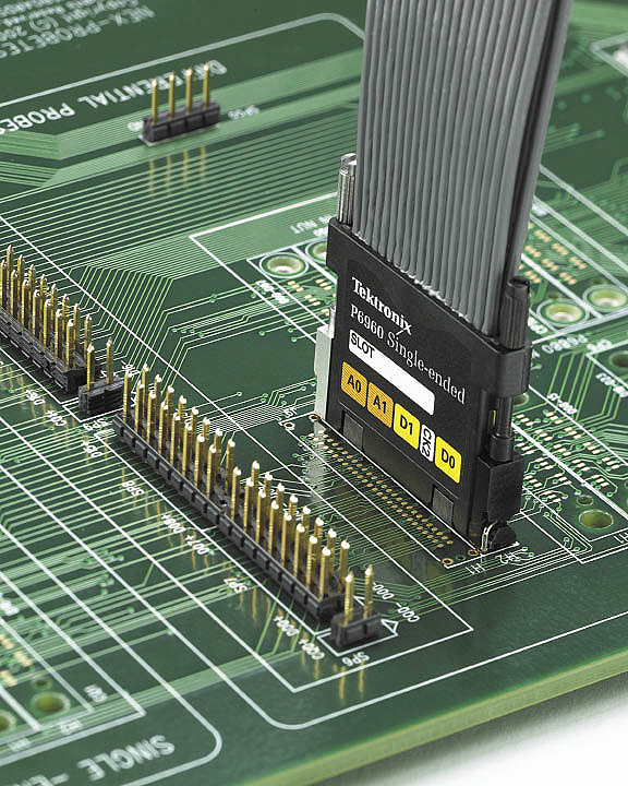
A logic analyzer’s probing scheme plays a critical role in high-speed digital acquisition. It’s critical that the probe delivers the signal to the logic analyzer with the highest possible fidelity. Some logic analyzers require separate probing connections for timing and state acquisitions. The technique “double probing,” can compromise the signal environment, affecting the actual measurements. For example, connecting two probes at once to the test point can create unacceptable levels of signal loading. Individual connections expose the test point to double the risk of damage or misconnection. Moreover, it is time-consuming to connect two probes. This simultaneous timing/state acquisition, speeds troubleshooting and supports signal integrity analysis tasks by minimizing the impact of probes on the DUT. The latest generation of probes can carry digital information to the logic analyzer, while delivering the same information as analog signals to an oscilloscope. Any pin of the probe can be used for both digital and analog acquisition. The analog signals route through the logic analyzer to an external oscilloscope, making it possible to determine, almost instantly, if a digital error is associated with an analog fault. A logic analyzer’s probes can also mount to dedicated connectors on the DUT. The location at which a bus is probed can make a difference in the appearance of the signals. Because of that, it’s preferable to place test connection points close to the receiving devices, where signals exhibit the characteristics that will be “seen” by the logic ICs.
Discuss this on The Engineering Exchange:

Tektronix
www.tektronix.com
Filed Under: ELECTRONICS • ELECTRICAL



Tell Us What You Think!